
The reduction of cost per component for many years was directly related to the reduction in feature size - dimensional scaling. But many other technology improvements made important contributions as well, such as increasing the wafer size from 2" all the way to 12".
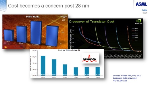
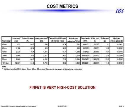
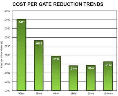
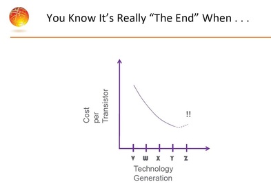
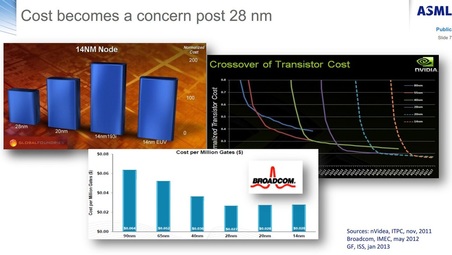
But many observers these days suggest that 28nm will be the optimal feature size with respect to cost for many years to come. Below are some charts suggesting so:
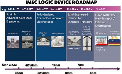
Looking at the other roadmap chart provided by IMEC and focusing on the SRAM bit cell in the first row, the situation seems far worse:
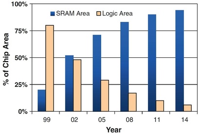
Unfortunately, most SoC die area is already dominated by SRAM and predicted to be so even more in the future, as illustrated by the following chart:
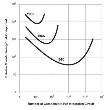
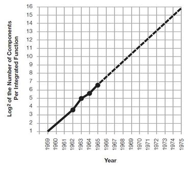
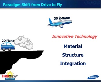
Dimensional scaling was not an integral part of Moore's assertion in 1965 – cost was. But dimensional scaling became the “law of the land” and, just like other laws, the industry seems fully committed to follow it even when it does not make sense anymore. The following chart captures Samsung’s view of the future of dimensional scaling for NV memory, and it seems relevant to the future of logic scaling just as well.






 RSS Feed