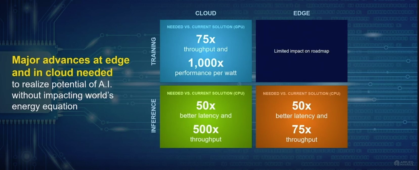
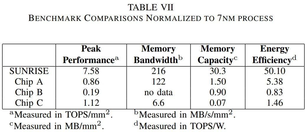
Helps understand the <1,000x AI computing achievement of Alibaba. 
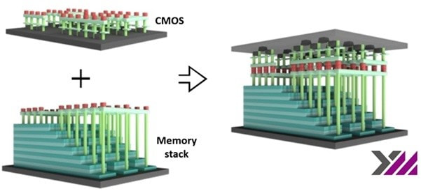
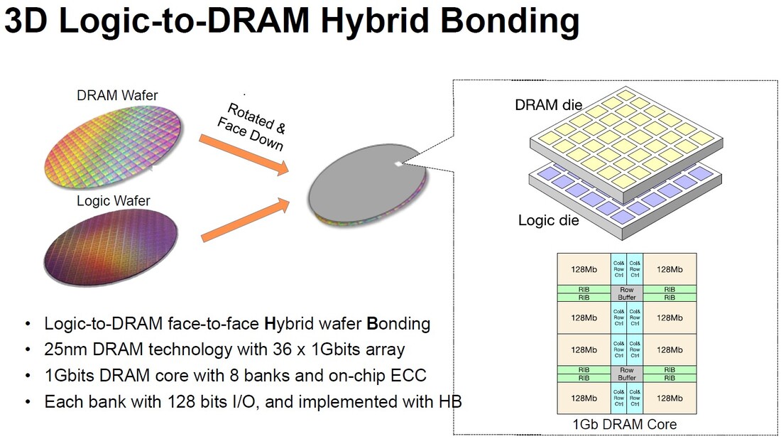
" Bonding stacked dies into a single package instead of a multiple package on a PCB increases I/O density by 100x.The energy-per-bit transfer can be reduced to 30x with the latest technology."
0 Comments
Demonstrating:
Leveraging Hybrid Bonding as an Alternative to Dimensional Scaling The technology driver for the next decade is AI. Quoting Applied Materials CEO Gary Dickerson “Are we ready for the biggest opportunity of our lifetime?” - “Gary’s been traveling the world talking to chipmakers and policymakers about a $10 trillion question: how do we capture the economic opportunity of AI, which will transform nearly every industry and institution over the coming years?” Gary presented the chart below presenting the 1,000x challenge to the semiconductors industry. Fig. 1: The required improvement in power-performance, to support the demand of AI computing. In fact the AI challenge is a moving target, as computing demands are growing by 2X about every 3.5 months. Fig. 2 Uri Frank, Google VP Engineering at ChipEx 2021. In recent years, there has been a buildup of tension in the US-China relation resulting in the US blocking China from securing access to advanced semiconductor technology and equipment. This includes access to advanced lithography tools such EUV. Accordingly, it was reported that only TSMC, Samsung and Intel have stayed in the race at technology node scaling below 10nm. Hence, it makes sense for Chinese firms to focus alternative resources on mature chip tech, say analysts. This could explain the adoption of hybrid bonding as a core technology by multiple Chinese corporations. Hybrid bonding allows them to replace dimensional node scaling with system-level 3D scaling. In August 2018, YMTC officially launched its ground-breaking Xtacking® architecture at the Flash Memory Summit, and won the “Best of Show” award. For its 3D NAND product, it uses two semiconductor manufacturing lines, one for the 3D NAND multi-level memory, and one for the peripheral (memory control) circuits as illustrated in Fig. 3 below. Fig. 3 Xtacking – using hybrid bonding to stack periphery on top of the 3D NAND memory fabric In September 2020 another Chinese company, IC League, published the results of their Heterogeneous Integration Technology on Chip (HITOC) Technology, an AI oriented IC development, in a paper titled Breaking the Memory Wall for AI Chip with a New Dimension . Fig. 4 IC League’s Heterogeneous Integration on Chip (HITOC) Technology Quoting from the paper: “With HITOC, we have two wafers, logic wafer, and memory wafer, bonded (using Hybrid Bonding) together [Fig. 4]. On the logic wafer, we have pools of processing units. Underneath the logic pool on the other wafer are pools of DRAM arrays.” The results reported by IC League were of better than orders of magnitude of overall improvement as could be seen in the table below. Fig. 5 HITOC technology the Sunrise device vs. conventional 2D alternative devices Last week at ISSCC 2022, Alibaba presented a more than 1,000 x improvement for AI computing devices using Hybrid Bonding in a paper titled “184QPS/W 64Mb/mm2 3D Logic-to-DRAM Hybrid Bonding with Process-Near- Memory Engine for Recommendation System.” The paper rightly points out that for AI computing data transfer dominates the system performance and power consumption. Consequently, overcoming the “Memory Wall” is key for AI computing and even more so with the rapid escalation of the size of the AI model computation requirements as illustrated in Fig. 6 below. Fig. 6 Escalation of AI module size compared to logic and memory annual technology improvements. The paper details the device architecture which leverages Hybrid Bonding to connect from the multi-bank DRAM directly to the AI processors’ logic. A die size of DRAM in commodity market is fairly tiny such as smaller than 50 mm2 in part due to higher yield and constraint of JEDEC standard. Interestingly, Alibaba’s logic-to-DRAM 3D chip is truly large chip; 602.22 mm2. By doing so, an important aspect of this work was to architect the logic and the corresponding DRAM as a full system design with multiple DRAM banks directly connecting to the multi cores logic underneath. Then, we can even extend this 3D Logic-to-DRAM concept in full wafer scale chip like Cerebra’s Wafer-Scale-Engine (CS-2). Unfortunately, Cerebras wafer-scale-engine is currently using only SRAM. Imagine what if a fully DRAM wafer would be directly hybrid bonded on Cerebra’s wafer scale engine. The company disclosed that their CS-2 has 40 gigabytes of on-chip SRAM. At the same size, DRAM can easily offer easily greater than 1 terabyte or at least 25 times greater capacity. Now, we are a step closer to breaking memory wall. Fig. 7 Illustration of system integration flow and the high level architecture Alibaba’s paper title suggests that the work targets the AI segment of Recommendation Systems, in which Alibaba has a high interest and has been developing systems including publishing work since at least 2017. This paper presents a very important breakthrough in performance and power reduction. Quoting from the paper: “"Compared to the CPU-DRAM system, our chip achieves 9.78× speedup. Note that the throughput and memory capacity can be further improved by scaling up the number of hybrid bonding blocks or using more advanced process technologies to serve more complicated recommendation models. In terms of energy efficiency, which is significant in memory-bound applications, our work achieves 184.11QPS/W (QPS – Queries per Second), which outperforms the CPU-DRAM system by 317.43×. In terms of area efficiency, the high-density hybrid bonding improves QPS/mm2 by 660×." The results were achieved while using a relatively old process node of 55 nm for the logic and were compared with the top of the line Intel Xeon Gold CPU processed at 14 nm. Fig. 8 Hybrid Bonding performance and energy improvements presented at ISSCC 2022. These results are multiple orders of magnitude better than the result reported by AMD for their V-Cache using hybrid bonding for added cache memory to their Ryzen CPU. There could be few reasons for the difference including the effort in re-architecting the system to highly leverage the Hybrid Bonding technology. The Alibaba chip was certainly architected from the ground up anticipating hybrid bonding, where the AMD combination may have been an afterthought. Further it should be noted that while AMD reported utilizing a vertical connectivity pitch of 9µm, the Chinese vendors are reporting vertical pitch of 3µ and in some cases even 1µ. The Sputnik Surprise – On February 7, 1958, the US established DARPA “to keep that technological superiority in the hands of the United State”, this is even more important now as we consider the potential power of AI technologies for the coming years.
|
Search Blog
Meet the BloggersFollow usRecommended LinksRecommended Blogs
Archives
July 2024
Categories
All
|