Monolithic 3D RC-JLT – Recessed-Channel Junction-Less Transistor
Follow link for presentation on: Detailed RCJLT Flow.
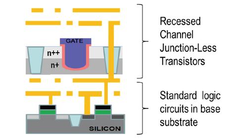
Monolithic 3D RC-JLT – Recessed-Channel Junction-Less Transistor
TechnologyMonolithic 3D IC technology is applied to producing monolithically stacked low leakage Recessed Channel Junction-Less Transistors (RC-JLTs).
Junction-less (gated resistor) transistors are very simple to manufacture, and they scale easily to devices below 20nm:
Superior contact resistance is achieved with the heavier doped top layer. The RCAT style transistor structure provides ultra-low leakage. Monolithic 3D IC provides a path to reduce logic, SOC, and memory costs without investing in expensive scaling down. |
Benefits
|
RC-JLT flow
Create a layer of Recessed Channel Junction-Less Transistors (RC-JLTs), a junction-less version of the RCAT used in DRAMs, by activating dopants at ~1000C before wafer bonding to the CMOS substrate and cleaving, thereby leaving a very thin doped stack layer from which transistors are completed, utilizing less than 400C etch and deposition processes.

Layer Transfer Technology (“Ion-Cut”) Defect-free single crystal obtained @ <400C
Leveraging a mature technology (wafer bonding and ion-cleaving) that has been the dominant SOI wafer production method for over two decades.
Innovate and create multiple thin (10s – 100s nanometer scale) layers of virtually defect free Silicon by utilizing low temperature (<400C) bond and cleave techniques, and place on top of active transistor circuitry. Benefit from a rich layer-to-layer interconnection density.
