Leveraging Hybrid Bonding as an Alternative to Dimensional Scaling
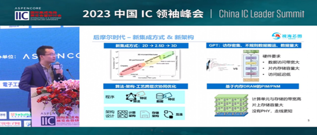
During the 2023 China IC Leaders Summit, Seehi founder Xu Dawen gave a speech entitled "DRAM Storage and Computing Chips: Leading the Revolution of AI Large-Scale Computing Power." The company has published the speech on its website, and we have selected some of the key statements from it.
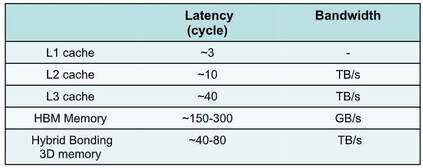
“From the trend of AI development and restricted hardware, it can be seen that the scale of AI models increase by more than one order of magnitude every 2-3 years, and the peak computing power of chips increases by an average of 3 times every two years, lagging behind the development of AI models . However, memory performance lags behind even more, with an average increase of 80% in memory capacity every two years, a 40% increase in bandwidth, and almost no change in latency.”
“Through 3D stacking technology, we can achieve the distance between the processor and DRAM to the micron level or even sub-micron level. In this case, the wiring is very short and the delay is relatively small. Through this technology, thousands or even hundreds of thousands of interconnection lines can be completed per square millimeter, achieving higher bandwidth. In addition, eliminating the PHY and shorter wiring will result in lower power consumption and better cost performance. The entire chip is composed of multiple tiles, and each tile is stacked by DRAM and logic. The DRAM part is mainly to provide high storage capacity and high transmission bandwidth, and the logic part is mainly to do high computing power and efficient interconnection. The NoC communicates between the tiles. This NoC is an in/through NoC design. It is interconnected with adjacent tiles on the same plane and communicates with the memory in the vertical direction.”
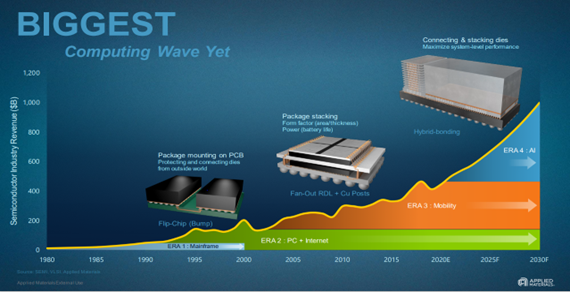
Undoubtedly, the US restrictions on state-of-the-art semiconductor equipment and computing chips have greatly impacted China's competitive position in the field of AI. However, it appears that some Chinese companies are now exploring alternative approaches, such as Hybrid Bonding and heterogeneous system integration. While this new path presents its own challenges, it offers unprecedented advantages. Delaying the adoption of this new approach could result in an insurmountable gap in the future. The following chart from Applied Materials illustrates this point clearly.


 RSS Feed