
We have a guest contribution from Zvi Or-Bach, the President and CEO of MonolithIC 3D Inc. Zvi's blog post is about Moore's Law and the impact of it on the industry today.
The assertion that Moore made in April 1965 Electronics paper was:"Thus there is a minimum cost at any given time in the evolution of the technology. At present, it is reached when 50 components are used per circuit. But the minimum is rising rapidly while the entire cost curve is falling (see graph below)."
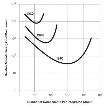
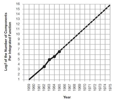
"The complexity for minimum component costs has increased at a rate of roughly a factor of two per year (see graph on next page). Certainly over the short term this rate can be expected to continue, if not to increase. Over the longer term, the rate of increase is a bit more uncertain, although there is no reason to believe it will not remain nearly constant for at least 10 years."
Clearly Moore's law is about cost, and Gordon Moore’s observation was that the optimum number of components (nowadays - transistors) to achieve minimum cost will double every year.
The reduction of cost per component for many years was directly related to the reduction in feature size - dimensional scaling. But many other technology improvements made important contributions as well, such as increasing the wafer size from 2" all the way to 12".
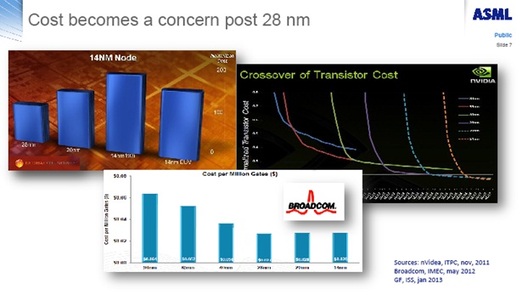
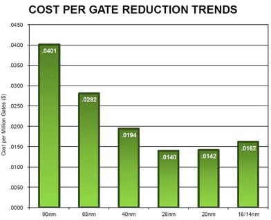
But many observers these days suggest that 28nm will be the optimal feature size with respect to cost for many years to come. Below are some charts suggesting so:
The reduction of cost per component for many years was directly related to the reduction in feature size - dimensional scaling. But many other technology improvements made important contributions as well, such as increasing the wafer size from 2" all the way to 12".
But many observers these days suggest that 28nm will be the optimal feature size with respect to cost for many years to come. Below are some charts suggesting so:
And more analytical work by IBS’ Dr. Handel Jones
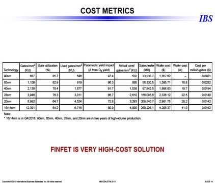
Graphically presented in the following chart
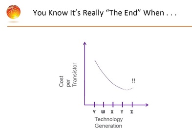
Or as nicely drawn by Globalfoundries
Recently EE Times reported that EUV Still Promising on IMEC's Road Map. IMEC provided a road map to transistor scaling all the way to 5nm, as illustrated in the following chart:
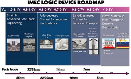
Yes, we probably can keep on scaling but, clearly, at escalating complexity and with completely new materials below 7nm. As dimensional scaling requires more advanced lithography it is clear that costs will keep moving up, and the additional complexity of transistor structures and all other complexities associated with these extreme efforts will most likely drive the costs even higher.
Looking at the other roadmap chart provided by IMEC and focusing on the SRAM bit cell in the first row, the situation seems far worse:
Looking at the other roadmap chart provided by IMEC and focusing on the SRAM bit cell in the first row, the situation seems far worse:
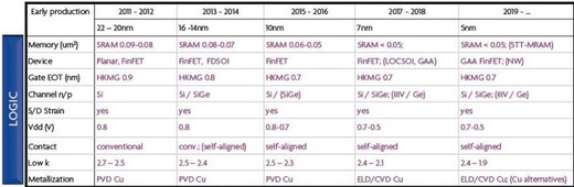
Since at 28 nm SRAM bit cell is already 0.081μm2, this chart indicates that future transistor scaling is barely applicable to the SRAM bit cell, which effectively is not scaling any more.
Unfortunately, most SoC die area is already dominated by SRAM and predicted to be so even more in the future, as illustrated by the following chart:
Unfortunately, most SoC die area is already dominated by SRAM and predicted to be so even more in the future, as illustrated by the following chart:
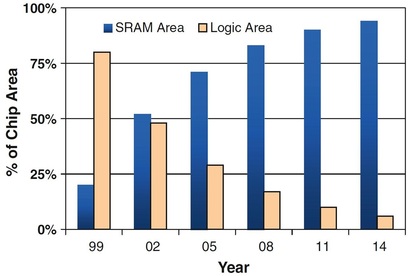
Source:. Y. Zorian, Embedded memory test and repair: infrastructure IP for SOC yield, in Proceedings the International Test Conference (ITC), 2002, pp. 340–349
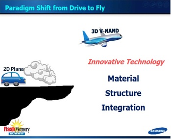
Dimensional scaling was not an integral part of Moore's assertion in 1965 – cost was. But dimensional scaling became the “law of the land” and, just like other laws, the industry seems fully committed to follow it even when it does not make sense anymore. The following chart captures Samsung’s view of the future of dimensional scaling for NV memory, and it seems relevant to the future of logic scaling just as well.
Dimensional scaling was not an integral part of Moore's assertion in 1965 – cost was. But dimensional scaling became the “law of the land” and, just like other laws, the industry seems fully committed to follow it even when it does not make sense anymore. The following chart captures Samsung’s view of the future of dimensional scaling for NV memory, and it seems relevant to the future of logic scaling just as well.


 RSS Feed