Monolithic 3D Inc., the Next Generation 3D-IC Company
  • Home
  • Technology
    • Technology
    • Papers, Presentations and Patents
    • Overview >
      • Background
      • Why Monolithic 3D?
      • Paths to Monolithic 3D
      • Applications
    • Ion-Cut: The Building Block
    • Monolithic 3D Logic >
      • RCAT
      • HKMG
      • Laser Annealing
      • RCJLT
      • 3D Embedded RAM
      • 3D Gate Array
      • FPGA
      • Ultra Large Integration - Redundancy and Repair
    • Monolithic 3D Memory >
      • 3D DRAM
      • 3D Resistive Memories
      • 3D Flash
    • Monolithic 3D Electro-Optics >
      • 3D Image Sensors
      • 3D Micro-Displays
  • 3D-IC Edge
    • 3D-IC Edge
  • News & Events
    • News & Events
    • S3S15 Game Change 2.0 Video/P
    • Webcast
    • Webinar
    • Press Releases
    • In the News
    • Upcoming Events
  • About Us
    • About Us
    • History
    • Team
    • Careers
    • Contact Us
  • Blog
  • Simulators

Please Help Me Understand IBM - Common Platform Technology Forum 2013

2/10/2013

3 Comments


"Innovations for Next Generation Scaling" 

Picture
We have a guest contribution from Zvi Or-Bach, the President and CEO of MonolithIC 3D Inc. Zvi discusses The Common Platform Technology Forum 2013.

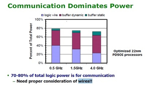
The 2013 Forum today (Feb 5, 2013) started with a presentation by Dr. Gary Patton, VP, IBM Semiconductor Research & Development Center. Gary very clearly articulated the two irresolvable challenges the industry now faces:

  • On chip interconnect
  • Lithography
These two challenges connect very well with our recent blog IEDM 2012 - The Pivotal Point for Monolithic 3D IC. Gary showed both the exponential increase of RC which results from the dimensional scaling of copper below 100nm width and the high cost associated with double and quad patterning. In addition, he showed how the extreme scaling of the copper metallization creates reliability challenges such as fatal EM modes, and scaling of the insulator k breeds TDDB and strength issues. As a reminder, in the recent IEDM (Dec. 2012) short course, IBM presented the following slide indicating that interconnect now dominates device power!
Picture
L. Chang, D.J. Frank - IEDM 2012 Short Course – IBM Watson Research Center
Gary also presented a multi-decade past to future slide that resembles the one presented here below. The decade ending at the year 2000 was the good old days of easy scaling of planar transistor, which he called the gate oxide limit. Then the industry followed with a decade of "Material Innovation" that he called the planar device limit, and starting in 2010 is the beginning of the "3D Era" - 3D transistors and stacked devices.
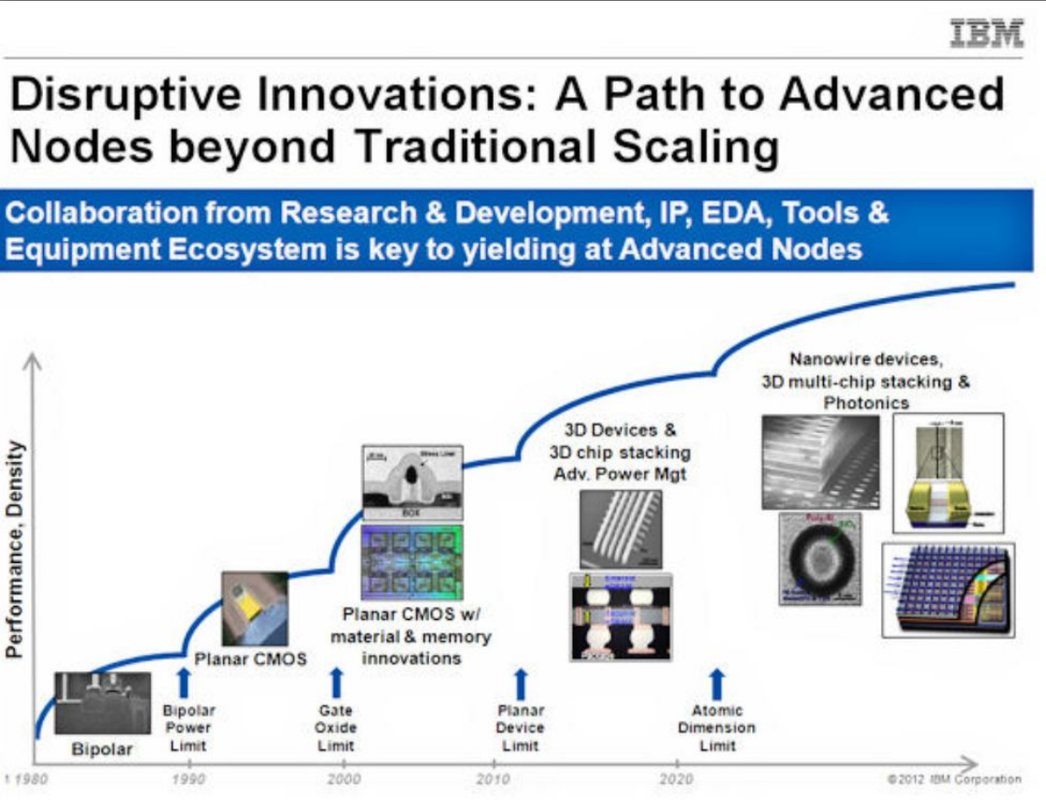
Picture
Figure 2
Finally he shared with us his vision of 3D devices with three planes of devices:

  • Logic Plane
  • Memory Plane
  • Photonic Plane
A vision we mutually share.

Now, here is my failure to understand. As a company who has been in the forefront of 3D and TSV research, IBM is well aware of the severe limitations of TSV as an alternative for vertical interconnect. The following cross-sectional picture by IBM, presented at the recent GSA Summit, clearly illustrates how large a TSV is in comparison to an interconnect via.
Picture
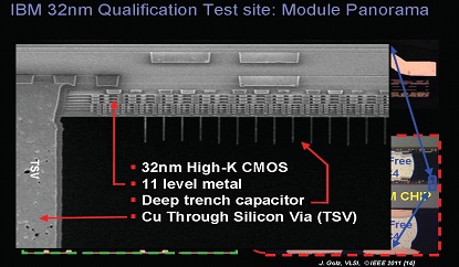
IBM Systems and Technology Group – GSA Silicon Summit 2012 (S.s lyer) – 2012 IBM Corporation
With TSVs of 5 micron diameters (and pitches of 15 micron due to keep out zones from stress issues) vs. vias of less than 50 nm, the ratio in vertical connectivity is 1:10,000 as illustrated in the following chart by Perinne Batude of CEA Leti.
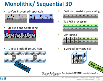
Picture
Figure 4
Clearly IBM technologists are well aware of the many research papers showing that TSVs, with their relatively huge size compared to all the other on-chip elements, diminish the performance or power benefits in folding designs to 3D. For example, the chart below was presented by Kim at the 2011 IEEE International Interconnect Technology Conference. The chart illustrates the performance benefits of folding a design twice (4 tiers of transistors) as dependent on the via size. At a via size of 5 microns there are actually no benefits, while at a via size of 0.1 micron the benefits are the equivalent of two nodes of dimension scaling!!!

Picture
Figure 5
So can someone please explain to me how come IBM is still talking about TSV as if it is the only representative of the "3D Era"???

And particularly now, when monolithic 3D is finally practical, and the NAND Flash memory vendors are adopting it across the board!?

submit to reddit
3 Comments

    Search Blog


    Meet the Bloggers


    Follow us


    To get email updates subscribe here:


    Recommended Links

    3D IC Community
    3D IC LinkedIn Discussion Group

    Recommended Blogs

    • 3D InCites by Francoise von Trapp
    • EDA360 Insider by Steve Leibson
    • Insights From the Leading Edge by Phil Garrou
    • SemiWiki by Daniel Nenni, Paul Mc Lellan, et al.

    Archives

    March 2022
    December 2021
    August 2021
    August 2018
    July 2018
    May 2018
    October 2017
    September 2017
    December 2016
    September 2016
    August 2016
    November 2015
    October 2015
    September 2015
    July 2015
    June 2015
    May 2015
    April 2015
    March 2015
    February 2015
    October 2014
    September 2014
    August 2014
    July 2014
    June 2014
    May 2014
    April 2014
    March 2014
    February 2014
    January 2014
    December 2013
    November 2013
    October 2013
    September 2013
    August 2013
    July 2013
    March 2013
    February 2013
    January 2013
    December 2012
    November 2012
    October 2012
    August 2012
    June 2012
    May 2012
    April 2012
    March 2012
    February 2012
    January 2012
    December 2011
    November 2011
    October 2011
    September 2011
    August 2011
    July 2011
    June 2011
    May 2011
    April 2011
    March 2011

    Categories

    All
    3d Design And Cad
    3dic
    3d Ic
    3d Nand
    3d Stacking
    3d Technology
    Brian Cronquist
    Dean Stevens
    Deepak Sekar
    Dram
    Education
    Heat Removal And Power Delivery
    Industry News
    Israel Beinglass
    Iulia Morariu
    Iulia Tomut
    Monolithic3d
    Monolithic 3d
    MonolithIC 3D Inc.
    Monolithic 3d Inc.
    Monolithic 3d Technology
    Moore Law
    Outsourcing
    Paul Lim
    Repair
    Sandisk
    Semiconductor
    Semiconductor Business
    Tsv
    Zeev Wurman
    Zvi Or Bach
    Zvi Or-Bach

    RSS Feed

© Copyright MonolithIC 3D Inc. , the Next-Generation 3D-IC Company, 2012 - All Rights Reserved, Patents Pending