Monolithic 3D Technology
- For logic applications, benefits similar to conventional scaling can be obtained with Monolithic 3D Scaling by leveraging existing fab equipment. For example, at the 22nm node, one folding (two stacked layers) will yield 2x lower power, 2x smaller silicon area, 4x smaller footprint, with only a fraction ($200M) of a typical new wafer-fab capital investment.
- Path 1 to Monolithic 3D: Construct recessed channel transistors in single crystal silicon, common in DRAM manufacturing, above copper interconnects at <400C.
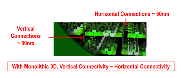
- Path 2 to Monolithic 3D: Employ any state-of-the-art replacement gate transistor, along with repeating layouts and a novel alignment scheme, to obtain a high density of vertical connections. The advantage of this technique is its use of state-of-the-art transistor technologies.
- Monolithic 3D enables a broad base of semiconductor companies to compete in creating and driving future generations of portable devices such as smart-phones and tablet computers.

