 | We have a guest contribution from Zvi Or-Bach, the President and CEO of MonolithIC 3D Inc. For over 4 decades the gap between computer processing speed and memory access has grown at about 50% per year, to more than 1,000x today. This provides an excellent opportunity to enhance the single-core system performance. An innovative 3D integration technology combined with re-architecting the integrated memory device is proposed to bridge the gap and enable a 1,000 x improvement in computer systems. |
ABSTRACT
For over 4 decades the gap between computer processing speed and memory access has grown at about 50% per year, to more than 1,000x today. This provides an excellent opportunity to enhance the single-core system performance. An innovative 3D integration technology combined with re-architecting the integrated memory device is proposed to bridge the gap and enable a 1,000 x improvement in computer systems. The proposed technology utilizes processes that are widely available and could be integrated in products within a very short time.
Keywords—processor-memory gap; 3D memory;
1. INTRODUCTION
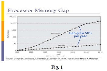
The Fig. 1 illustrates the growing gap between processing and memory access [1,2]
The Fig. 1 illustrates the growing gap between processing and memory access [1,2]
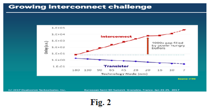
The source for this gap is directly related to the gap between transistor performance progress vs. on-chip interconnect delay as illustrated in Fig. 2 [3,4]
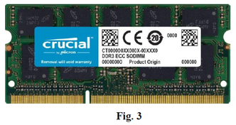
In most computer systems the processor is being bought from a processor vendor (Intel, AMD, Nvidia,…) while the memory is being bought from memory vendors (Micron, Samsung, Hynix,…). In many cases multiple memory devices are being integrated into a memory module, often called DIMM (such as Fig. 3), which is then integrated into a computer system with the processor(s). This integration is driven by the very different semiconductor technology knowhow, and manufacturing infrastructure required, for processors vs. memories.
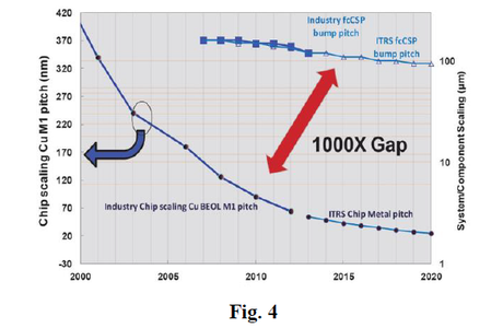
Printed circuit board (‘PCB’) is used to connect processor to memory adding significantly to the ‘gap,’ as illustrated in Fig. 4 [5]
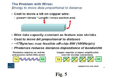
This gap has been articulated in many forms including in a presentation titled “Why we need Exascale and why we won't get there by 2020” [6] which included Figs. 5. There is a tremendous power cost in moving data to and from an off-chip memory, and even an ‘integrated’ memory.
2. PREVIOUSLY PROPOSED SOLUTIONS
A joint research by teams from Stanford University, Berkeley and Carnegie Mellon was summarized in their paper “Energy-Efficient Abundant-Data Computing: The N3XT 1,000×” illustrated in Fig. 6 [7].
A joint research by teams from Stanford University, Berkeley and Carnegie Mellon was summarized in their paper “Energy-Efficient Abundant-Data Computing: The N3XT 1,000×” illustrated in Fig. 6 [7].
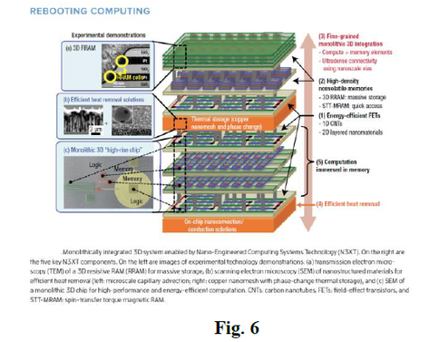
Yet it is very unclear if and when any of the proposed new technologies – CNT, RRAM, STT-MRAM - would be available and in high volume production and ready to be used for manufacturing of computer systems.
3D integration using TSV has been considered as another attractive option to bridge the gap. A paper by D. H. Woo concluded “On average, for single-threaded memory intensive applications, the speedups range from 1.53 to 2.14 compared to a conventional 2D architecture” [8]. This is far less than the monolithic 3D work done by Stanford. In Fig. 12 Micron provides a chart comparing TSV vs. DDR3. Micron has formed an industry consortium named Hybrid Memory Cube – “HMC,” to leverage TSV for bridging the memory gap.
3D integration using TSV has been considered as another attractive option to bridge the gap. A paper by D. H. Woo concluded “On average, for single-threaded memory intensive applications, the speedups range from 1.53 to 2.14 compared to a conventional 2D architecture” [8]. This is far less than the monolithic 3D work done by Stanford. In Fig. 12 Micron provides a chart comparing TSV vs. DDR3. Micron has formed an industry consortium named Hybrid Memory Cube – “HMC,” to leverage TSV for bridging the memory gap.
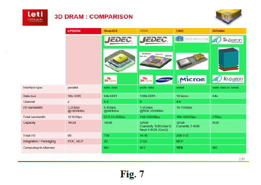
A table comparing 2.5D and TSV memory stacking technologies is presented in Fig. 7.
While the various approaches offer clear performance improvements, they are far from what is suggested by the N3XT factor of 1,000x. It would seem that the inherent limitations (density, delay) of the TSV technology are the limiting factors. We therefore propose a novel 3D integration that offers more than 1,000x better vertical connectivity to enable comprehensive bridging of the processor memory gap, while still utilizing widely available commercial processes that make it attractive for fast industry adoption.
While the various approaches offer clear performance improvements, they are far from what is suggested by the N3XT factor of 1,000x. It would seem that the inherent limitations (density, delay) of the TSV technology are the limiting factors. We therefore propose a novel 3D integration that offers more than 1,000x better vertical connectivity to enable comprehensive bridging of the processor memory gap, while still utilizing widely available commercial processes that make it attractive for fast industry adoption.
3. BRIDGING THE GAP WITH MONOLITHIC 3D INTEGRATION
In TSV technology the layer thickness of each layer in the stack is tens of microns (~50 μm) and the via through each stacked layer is about 5 microns in diameter. Monolithic 3D integration enables stacked layers of tens of nanometers (~50 nm) with vias that are of similar size of regular vias between metal layers. All currently known 3D integration techniques that provide such vertical connectivity require major process and equipment changes at the wafer fab. The following approach is a monolithic 3D innovation that overcomes this challenge.
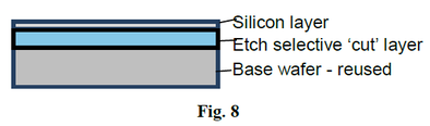
Or-Bach in “Modified ELTRAN® - A Game Changer for Monolithic 3D” presented a 3D integration that does not require process change but would require a special porous base substrate [9]. Here we propose an alternative substrate could be far more readily available (Fig. 8).
In TSV technology the layer thickness of each layer in the stack is tens of microns (~50 μm) and the via through each stacked layer is about 5 microns in diameter. Monolithic 3D integration enables stacked layers of tens of nanometers (~50 nm) with vias that are of similar size of regular vias between metal layers. All currently known 3D integration techniques that provide such vertical connectivity require major process and equipment changes at the wafer fab. The following approach is a monolithic 3D innovation that overcomes this challenge.
Or-Bach in “Modified ELTRAN® - A Game Changer for Monolithic 3D” presented a 3D integration that does not require process change but would require a special porous base substrate [9]. Here we propose an alternative substrate could be far more readily available (Fig. 8).
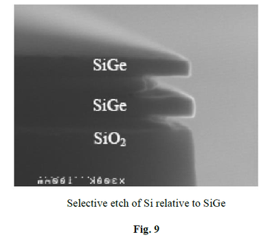
Epitaxial wafer with silicon over SiGe are already the preferred substrates of future nodes for silicon nano-wires, with gate-all-around in which the SiGe layer is used as a sacrificial layer. We suggest a reverse use of such epitaxial layer, in which the SiGe would function as an etch-selective ‘cut’ layer by functioning as an etch stop for a back grinding and etch-back process sequence. The 3D technique of flip, bond and etch-back of an SOI donor had been practiced by MIT Lincoln Lab for many years [10, 11]. Use of a SiGe ‘cutable’ substrate is an attractive alternative as SOI wafers are quite expensive. The SiGe ‘cutable’ substrate could be processed as a regular wafer through the fab all through the process, including BEOL interconnection layers. Then it could be flipped over and bonded to a target wafer. A simple grind and etch-back operation using the SiGe layer an etch stop follows, which could be later removed by a follow-up etch step. Accordingly, the transferred layer could be made as thin as desired, down to less than 100 nm of silicon, removing by grinding and etch back almost all of the 700 micron of the original substrate. Fig. 16 illustrates selective etching of silicon allowing SiGe to serve as an etch stop [12, 13, 14].
Currently available production worthy wafer bonders can support such layer transfers with less than 200nm (3σ) misalignment [15].
This fine grained 3D integration could be used for reengineering memory product into two strata, one for arrays of bit cells and one for memory control circuitry, as is illustrated in Fig. 10.
This fine grained 3D integration could be used for reengineering memory product into two strata, one for arrays of bit cells and one for memory control circuitry, as is illustrated in Fig. 10.
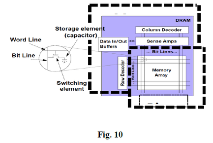
Such densely connected 3D partitioning would reduce memory costs as bit-cell processing is completely disconnected and different from memory control circuitry processing. Manufacturing memory and logic on separate wafers would reduce overall costs, while enabling a paradigm shift in the logic and memory interface.
Having the memory peripheral circuitry not in the periphery of the device but rather on top of it, allows cost effective breaking up of the memory array into an array of small memory units, such as 200 μm x 200 μm units, each with its own word-lines and bit-lines.
Additionally, multiple memory strata could be vertically integrated to offer much larger memory capacity for the same footprint. Fig. 11 illustrates a region of such memory strata having two adjacent memory units with word-lines or bit-lines traveling in-between, and a per-layer selector, and nano-pads for vertical connectivity.
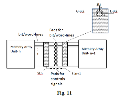
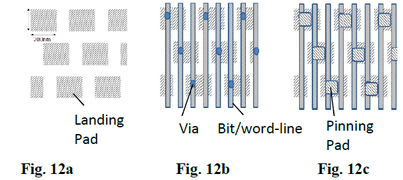
Fig. 12a illustrates a vertical connectivity region having landing pads large enough to cover the bonding misalignment. Fig. 12b illustrates the region with overlaying via connecting these pads to the word-lines or the bits-lines, and Fig. 12c illustrates the overlying pinning pads.
Memory strata could be constructed by integrating such connectivity structure with the block diagram of Fig. 11 to form a stackable memory structure, which could be produced as a generic memory substrate. Hybrid wafer bonding could be used to provide vertical connectivity between layers in the stack. The required distance between two adjacent units (Fig. 11) could be less than 1 μm, resulting in less than 0.5% overhead for this 3D memory tiling and connectivity structure.
Fig. 13 illustrates a vertical cross-section view of 4 strata distributing the top select signal to each stratum in the stack.
This connectivity structure opens up many usage options, including redundancy to overcome defects. The memory is constructed by stacks of strata, each constructed as array of units connected in parallel with a select signal per stratum. One of these strata could serve as a redundancy stratum with per unit select allowing repair at the unit level. In addition, multiple memory access options could be enabled from high speed local access to a global—albeit somewhat slower—access to large array of units. An additional advantage of this architecture is having one (or two) memory control strata to service multiple memory strata.
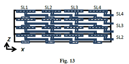
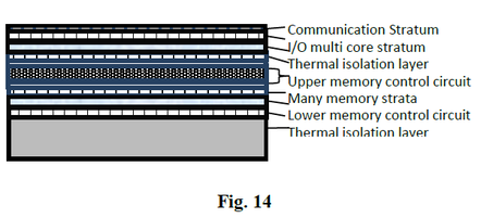
Fig. 14 illustrates a 3D computer system utilizing the technologies presented here. The base silicon is a carrier substrate which also provides cooling to the main multi-core computing stratum. Through the first thermal isolation layer, the computer stratum is connected to the multi-unit lower memory control stratum, which controls the multi-unit memory array strata. Overlaying the memory strata is an upper memory control stratum which provides a second access to the same memory strata. Through a second thermal isolation layer a second computing stratum could be connected to the upper memory control stratum. The second computing stratum could be the Input/Output computing stratum communicating with external devices utilizing another communications stratum. The communications stratum could utilize wired, wireless, optical or other channels to communicate with external devices. An upper heat removal apparatus could overlay the communications stratum.
4. SUMMARY
We have presented a 3D integration technology combined with memory architecture that could utilize existing processes and infrastructure to bridge the processor memory gap. Using these concepts would enable the current connectivity of about 100 wires at average 20 mm length to be replaced with 100,000 wires with average 20 μm length, with the corresponding 1,000x improvements in computation speed, power, and cost. Additional advantages would be reduction of overall system costs, establishing a generic memory fabric with build in full repair capability at factory and field.
We have presented a 3D integration technology combined with memory architecture that could utilize existing processes and infrastructure to bridge the processor memory gap. Using these concepts would enable the current connectivity of about 100 wires at average 20 mm length to be replaced with 100,000 wires with average 20 μm length, with the corresponding 1,000x improvements in computation speed, power, and cost. Additional advantages would be reduction of overall system costs, establishing a generic memory fabric with build in full repair capability at factory and field.
5. REFERENCES
[1] Hennessy, John L. and David A. Patterson. Computer Architecture: A Quantitative Approach. 4th ed., p. 289. Elsevier, 2007.
[2] McCalpin, John D. “Memory Bandwidth and System Balance in HPC Systems”, Invited Talk, International Conference for High Performance Computing, Networking, Storage, and Analysis, 2016.
[3] Wu, Banqiu, and Ajay Kumar. "Extreme ultraviolet lithography and three dimensional integrated circuit—A review." Applied Physics Reviews 1.1, 2014.
[4] Yeap, Geoffrey. "Smart mobile SoCs driving the semiconductor industry: Technology trend, challenges and opportunities." In Electron Devices Meeting (IEDM), 2013.
[5] Sun, Jack Y-C. "System scaling and collaborative open innovation." VLSI Technology (VLSIT), 2013 Symposium on. IEEE, 2013.
[6] Simon, Horst. "Why we need Exascale and why we won’t get there by 2020." Optical Interconnects Conference, Santa Fe, New Mexico. 2013.
[7] Aly, Mohamed M. Sabry, et al. "Energy-efficient abundant-data computing: The n3xt 1,000 x." Computer 48.12 (2015): 24-33.
[8] Woo, Dong Hyuk, et al. "An optimized 3D-stacked memory architecture by exploiting excessive, high-density TSV bandwidth." High Performance Computer Architecture (HPCA), 2010 IEEE 16th International Symposium on. IEEE, 2010.
[9] Or-Bach, Zvi, et al. "Modified ELTRAN®—A game changer for Monolithic 3D." SOI-3D-Subthreshold Microelectronics Technology Unified Conference (S3S), 2015 IEEE. IEEE, 2015.
[10] Chen, C. K., et al. "3D-enabled heterogeneous integrated circuits." SOI-3D-Subthreshold Microelectronics Technology Unified Conference (S3S), 2013 IEEE. IEEE, 2013.
[11] Chen, C. K., et al. "SOI-enabled three-dimensional integrated-circuit technology." SOI Conference (SOI), 2010 IEEE International. IEEE, 2010.
[12] Orlowski, Marius, et al. "(Invited) Si, SiGe, Ge, and III-V Semiconductor Nanomembranes and Nanowires Enabled by SiGe Epitaxy." ECS Transactions 33.6 (2010): 777-789.
[13] Borenstein, J. T., et al. "Silicon germanium epitaxy: a new material for MEMS." MRS Proceedings. Vol. 657. Cambridge University Press, 2000.
[14] Taraschi, Gianni, et al. "Ultrathin strained Si-on-insulator and SiGe-on-insulator created using low temperature wafer bonding and metastable stop layers." Journal of The Electrochemical Society 151.1 (2004): G47-G56.
[15] Uhrmann, T. "Monolithic IC Integration-Key alignment specifications for high process yield." SOI-3D-Subthreshold Microelectronics Technology Unified Conference (S3S), IEEE. 2014.


 RSS Feed