
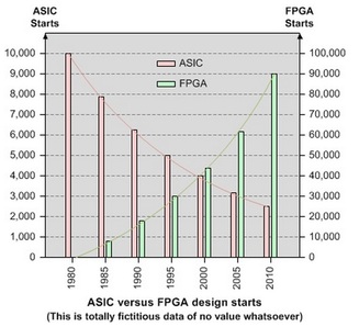
One would expect that such a trend would have a very positive effect on the FPGA market, as there is no mask-set cost associated with an FPGA design and, accordingly, far lower NRE costs per design. The following fictitious chart presented in the EE Times article: What’s the number of ASIC versus FPGA design starts?, illustrates these expectations.
In the following we will present our theory why it did not happen and some potential implications for the future.
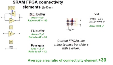
We believe that the stagnation of FPGA growth is mostly due to the inefficiency of the FPGA technology. Most FPGAs use SRAM as the programming or ‘switch’ technology. Interconnects are the dominating resource in modern designs. Within an SRAM based FPGA the programming of interconnects is implemented by an SRAM cell control of a pass transistor, driver, or bidirectional driver. The following chart illustrates the diffusion area associated for such Programmable Interconnect Cell (PIC) assessed in 45nm technology and compared to the size of mask-defined equivalent – the via. The results indicate that the cell area overhead for the SRAM PIC is over 30X when compared to a via, which does not include the additional circuit overhead area needed to program and control the SRAM PIC.
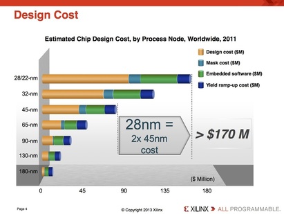
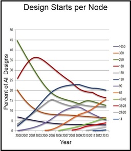
This high programmability overhead suggests that many of the current ASIC designs cannot be replaced by an FPGA design. Consequently, when advanced technology NRE is too high, the alternative is to use older node ASIC technologies. Since the number one driver for cost of mask-sets and NRE is the associated capital, the cost of older technologies goes down dramatically over time. The 30X area penalty means that one could use a node that is five generations older and have a competitive solution when compared to current node FPGA. Taking into account the 60% gross margin of the FPGA companies and the overhead of using a fixed-sized device of an FPGA family rather than a custom tailored Standard Cell device, these could compensate for an additional two nodes. Looking again at the design costs as illustrated in the Xilinx chart above, we can see that at 180 nm the design costs are pretty low and the mask set costs are too small even to register on the chart.
There are potentially many implications of this change in Moore’s Law. One of those implications could affect the future of FPGAs.
Traditionally FPGAs have been, and still are, a technology driver of new logic technology nodes. This early adoption gave the FPGA customer a constantly better programmable platform for their designs. Now that dimensional scaling does not provide better cost, it will result in a build-up of pressure for FPGA customers to use a depreciated technology node as an alternative. Over time designers would see the NRE of 65nm going down to about what the 180nm NRE is today. Comparing a 65nm Standard Cell design to an FPGA of 28nm suggests that far more designs could be better off with Standard Cell. As 20 nm and 14 nm FPGAs would not provide a better cost than the 28 nm one, it means that the FPGA market could see a growing challenge in the coming years.
Designers chose older nodes not just for its lower mask-set and NRE costs but also for availability of broader embedded options such as flash memories and analog cells. But those are becoming available on newer nodes over time as well. The 65 nm node is now ramping up and would become the preferred choice for new designs in a few years, as its mask-set cost and NRE keep going down thanks to deprecation and broader availability. As volume production of older designs winds down, vendors are reducing their costs to bring new designs in, and will soon make the 65 nm as easy to access as 180 nm is now. FPGA vendors will release newer products on 20nm and 14nm but those would not offer lower production costs than the 28 nm FPGA products and will be less and less competitive versus a ‘not too old’ technology node such as 65 nm. It only seems logical that these new semiconductor industry dynamics will have a negative effect on the FPGA market and a positive effect on ASIC and Structured ASIC technologies.
Thus it behooves us to consider what can the FPGA vendors do to keep their business growth.
Interestingly, the same trend that now works against FPGA technologies could be used to improve their competitiveness. In the early days two major FPGA technologies were competing in the market. The SRAM technology and the anti-fuse technology. The SRAM technology had higher switch overhead, but ended up winning because it benefitted from two major advantages. First, it did not need any major process changes and could be adapted to newer nodes as soon as those could be fabricated. Second was their ability to reprogram the device over and over again. Now that new process nodes do not provide lower costs, FPGA vendors could look to other than SRAM technology as a new path to improve their programmable platforms. As for anti-fuse, the significant effort in recent years to develop RRAM technology opens the possibility of adopting antifuse technology that could offer re-programmability. Even more important is the fact that re-programmability these days is far less important as all FPGA designs utilize simulation technology and other EDA tools, as the trial and error methodology no longer can be effectively used for modern designs.
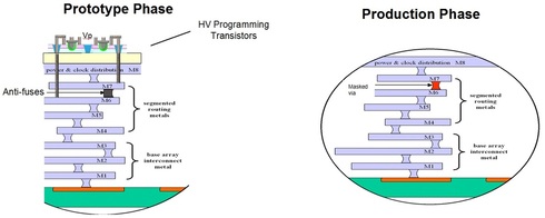
A special type of antifuse programmable technology could be most effective – Antifuse-based 3D High Density FPGA. This type of programmable fabric leverages anti-fuse metal to metal technology, which use 3D transistors for programming the anti-fuses. The 3D transistors could handle the higher voltage required for the programming and provide the interconnect programming with minimal device density impact. The 3D anti-fuse programmable fabric density is very similar to a via programmable fabric. Via programmable fabrics has been used with structured ASICs such as those offered by eASIC and Triad Semiconductors (ViASIC). They provide a programmable fabric with about a 2X area penalty vs. mask-defined standard cell technologies. These antifuses could be made as one time or reprogrammable devices and be fully replaced by mask-defined vias for even lower cost volume production, as illustrated by the following chart



 RSS Feed