Monolithic 3D Inc., the Next Generation 3D-IC Company
  • Home
  • Technology
    • Technology
    • Papers, Presentations and Patents
    • Overview >
      • Background
      • Why Monolithic 3D?
      • Paths to Monolithic 3D
      • Applications
    • Ion-Cut: The Building Block
    • Monolithic 3D Logic >
      • RCAT
      • HKMG
      • Laser Annealing
      • RCJLT
      • 3D Embedded RAM
      • 3D Gate Array
      • FPGA
      • Ultra Large Integration - Redundancy and Repair
    • Monolithic 3D Memory >
      • 3D DRAM
      • 3D Resistive Memories
      • 3D Flash
    • Monolithic 3D Electro-Optics >
      • 3D Image Sensors
      • 3D Micro-Displays
  • 3D-IC Edge
    • 3D-IC Edge
  • News & Events
    • News & Events
    • S3S15 Game Change 2.0 Video/P
    • Webcast
    • Webinar
    • Press Releases
    • In the News
    • Upcoming Events
  • About Us
    • About Us
    • History
    • Team
    • Careers
    • Contact Us
  • Blog
  • Simulators

Monolithic 3D High Performance (HKMG) Transistors

Follow link for presentation on: Detailed HKMG flow.
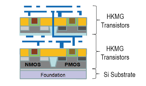
Picture

Technology

The monolithic 3D IC technology is applied to produce monolithically stacked high performance High-k Metal Gate (HKMG) devices, the world’s most advanced production transistors.

3D Monolithic State-of-the-Art transistors are formed with ion-cut applied to a gate-last process, combined with a low temperature face-up layer transfer, repeating layouts, and an innovative inter-layer via (ILV) alignment scheme.

Monolithic 3D IC provides a path to reduce logic, SOC, and memory costs without investing in expensive scaling down.

Benefits

  •  Maximum State-of-the-Art transistor performance on multi-strata
  •  2x lower power
  •  2x smaller silicon area
  •  4x smaller footprint
  •  Performance of single crystal silicon transistors on all layers in the 3DIC
  •  Scalable: scales normally with equipment capability
  •  Forestalls next gen litho-tool risk
  •  High density of vertical interconnects enable innovative architectures, repair, and redundancy

HKMG 3D Flow

Create a logic layer with any transistor that uses a replacement-gate process. Innovative alignment schemes, combined with repeating layouts, obtain sub-50nm, and hence dense, through-silicon electrical connections.
Picture
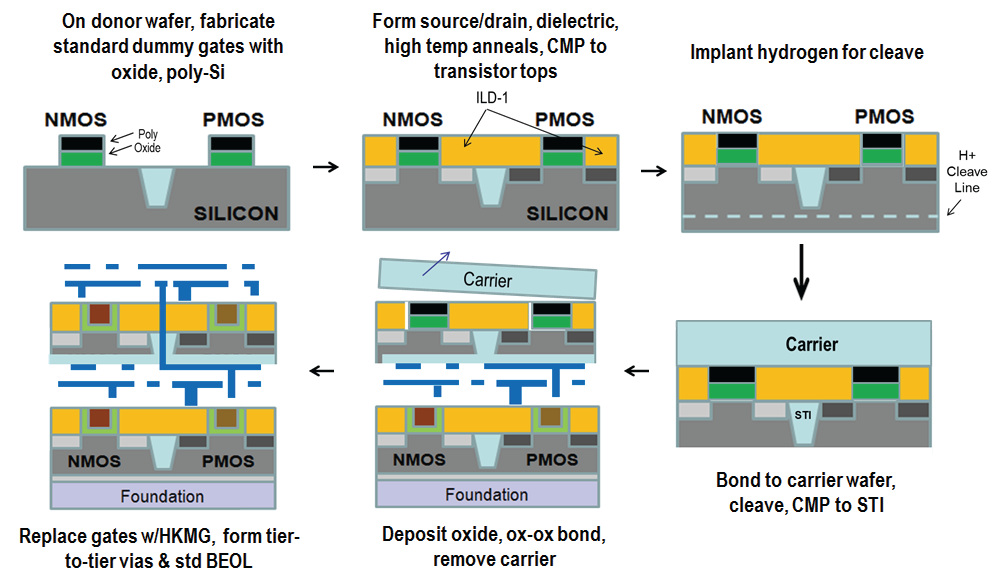
Layer Transfer Technology (“Ion-Cut”)Defect-free single crystal obtained @ <400C
Leveraging a mature technology (wafer bonding and ion-cleaving) that has been the dominant SOI wafer production method for over two decades.
Innovate and create multiple thin (10s – 100s nanometer scale) layers of virtually defect free Silicon by utilizing low temperature (<400C) bond and cleave techniques, and place on top of active transistor circuitry. Benefit from a rich layer-to-layer interconnection density.
Picture
© Copyright MonolithIC 3D Inc. , the Next-Generation 3D-IC Company, 2012 - All Rights Reserved, Patents Pending