Pulsed Laser Annealing: A scalable and practical technology for monolithic 3D IC
Two Major Semiconductor Trends Help Make Monolithic 3D Practical
As we have pushed dimensional scaling:
Much less mass to heat, and for much shorter time -> reduction in total thermal energy
- The volume of the transistor has scaled
- Processing temperatures have trended lower
Much less mass to heat, and for much shorter time -> reduction in total thermal energy
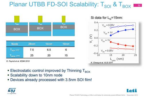
Source: LETI
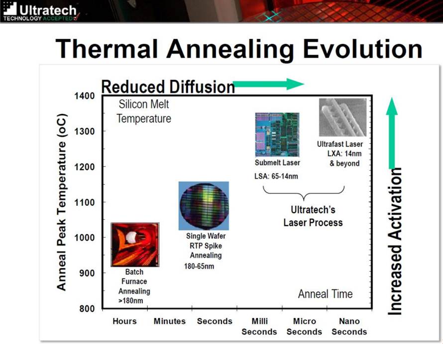
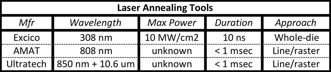
Annealing Trend with Scaling Source: Ultratech
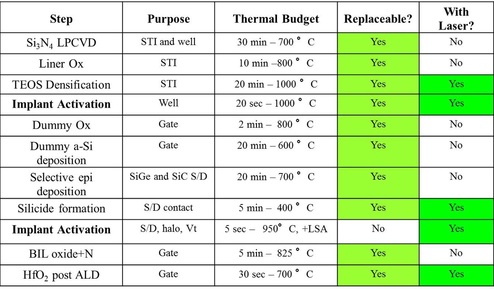
Major Thermal Process Steps
in a Modern IC Process
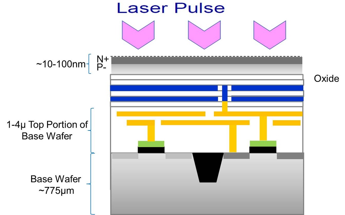
Laser Spike Annealing
- Goals
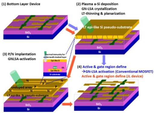
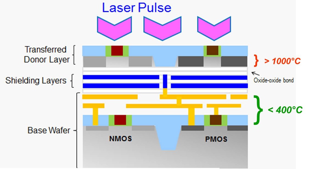
- Do not disrupt already-fabricated devices lying beneath the fresh Si layerIssues
- Thermal stress
- Heat transfer dynamics to underlying layers
- Approach
- Use combination of thermal/electrical insulators, and high heat capacity metallic shield layers
- All materials compatible with existing IC technology
Dopant Activation by Laser: IEDM 2013 Example
- Taiwan National Nano Device Laboratory: IEDM13-Paper #9.3
- “Researchers from Taiwan’s National Nano Device Laboratories avoided the use of TSVs by fabricating a monolithic sub-50-nm 3D chip, which integrates high-speed logic and nonvolatile and SRAM memories... The monolithic 3D architecture demonstrated high performance – 3 ps logic circuits, 1T 500ns nonvolatile memories and 6T SRAMs with low noise and small footprints…”
Dopant Activation by Laser:
IEDM 2013 Example
Laser Spike Annealing of Top Monocrystalline Silicon Layer
Types
|
Dwell time ~ 275µs |
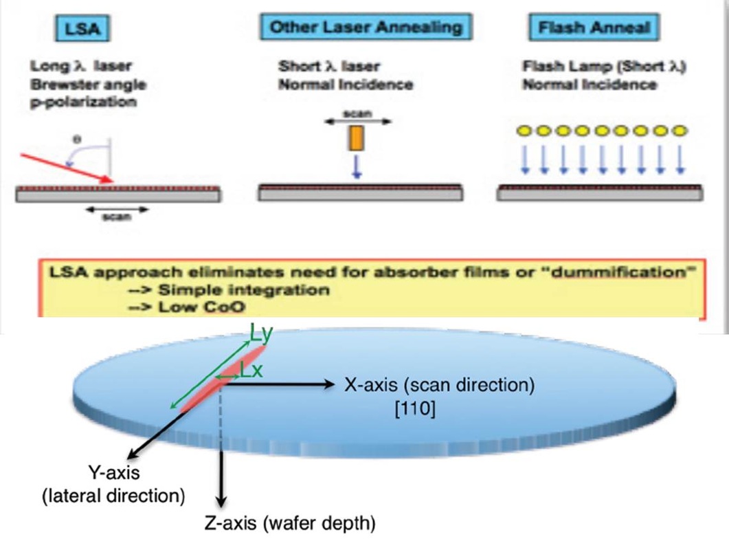
LSA 100A – Short Pulse, Small Spot
|
Laser Spike Annealing of Top Monocrystalline Silicon Layer
Ion-Cut Applied to Monolithic 3D

Pulsed Laser Anneal May Be Used to Repair Ion-Cut Lattice Damage of Top Monocrystalline Silicon Layer
Conclusions
- Monolithic 3D IC technology is a leading approach to extend IC scaling beyond the 7-10 nm nodes
- Use of laser spike annealing on a thin layer of c-Si, combined with metal and insulator thermal shield layers, allows:
- No disruption to underlying structures
- Annealing of ion-cut damage
- Densification and other anneals
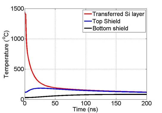
- Pulsed laser annealing works because:
- The thermal energy required is shielded from the underlying structures by the thermal heat capacity of the shield
References
- "Pulsed Laser Annealing: A scalable and practical technology for monolithic 3D IC", Paper presented at the 2013 IEEE 3DIC Conference, October 2013.
- "Thermal Considerations for Monolithic Integration of Three-Dimensional Integrated Circuits", Poster presented at the 2013 S3S Conference, October 2013.
- "Monolithic 3D Advantage", Free E-book, February 2013.
- "Monolithic 3D - In General", Free E-book, March 2013.
- Obtaining Monocrystalline Semiconductor Layers for Monolithic 3D, Blog post by Israel Beinglass, the CTO of MonolithIC 3D Inc.