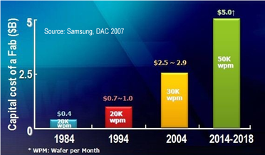
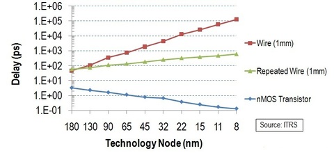
Monolithic 3D Inc., the Next Generation 3D-IC Company
  • Home
  • Technology
    • Technology
    • Papers, Presentations and Patents
    • Overview >
      • Background
      • Why Monolithic 3D?
      • Paths to Monolithic 3D
      • Applications
    • Ion-Cut: The Building Block
    • Monolithic 3D Logic >
      • RCAT
      • HKMG
      • Laser Annealing
      • RCJLT
      • 3D Embedded RAM
      • 3D Gate Array
      • FPGA
      • Ultra Large Integration - Redundancy and Repair
    • Monolithic 3D Memory >
      • 3D DRAM
      • 3D Resistive Memories
      • 3D Flash
    • Monolithic 3D Electro-Optics >
      • 3D Image Sensors
      • 3D Micro-Displays
  • 3D-IC Edge
    • 3D-IC Edge
  • News & Events
    • News & Events
    • S3S15 Game Change 2.0 Video/P
    • Webcast
    • Webinar
    • Press Releases
    • In the News
    • Upcoming Events
  • About Us
    • About Us
    • History
    • Team
    • Careers
    • Contact Us
  • Blog
  • Simulators


Background

Over the past 30 years, we have seen an exponential increase in the functionality and performance of Integrated Circuits. This has largely been due to Conventional Scaling, which entails a 30% reduction of feature sizes every 2 years. Hence, feature sizes have reduced from 2um in 1984 to 32nm in 2010, a factor of almost 150x! However, many difficult challenges loom on the horizon, which has led several industry heavyweights to question the future of conventional scaling. Read Scaling is dead, says IBM CTO, and Life after Moore's Law, by Bill Dally, the Chief Scientist of nVidia for more information.

Fig. 1 describes two of the key challenges that arise from conventional scaling:
  • While transistor performance improves with reduced feature sizes, interconnect performance degrades. Fig. 1(a) reveals that the gap between transistor delay and the delay of a representative 1mm wire has increased from 10x at the 180nm node to 10,000x at the 32nm process node [1] .It is possible to use repeaters (made of transistors) to speed up wires at the expense of silicon area and power - however, there still exists a 500x gap between transistor delay and repeated wire delay at the 32nm node. This gap between transistor and wire delay increases exponentially every generation, as shown in Fig. 1(a), causing tremendous challenges.
  • Reduced feature sizes require progressively more expensive wafer fab equipment. This has resulted in the capital cost for wafer fabs increasing from ~$400M for 2um technology to ~$4B for 32nm technology (Fig. 1(b)) [2]. Conventionally-scaled fabs have become prohibitively expensive for most companies in the industry today. IBS (2010) predicts that there will only be 4 players at the 20nm node.


3d ic
3d ic
                                                        (a)                                                                                                                         (b)

Figure 1: By-products from Conventional Scaling that are impacting the industry today (a) Ratio of Wire Delay to Transistor Delay increases exponentially (b) Capital Cost of a Fab increases exponentially.

© Copyright MonolithIC 3D Inc. , the Next-Generation 3D-IC Company, 2012 - All Rights Reserved, Patents Pending