Monolithic 3D Inc., the Next Generation 3D-IC Company
  • Home
  • Technology
    • Technology
    • Papers, Presentations and Patents
    • Overview >
      • Background
      • Why Monolithic 3D?
      • Paths to Monolithic 3D
      • Applications
    • Ion-Cut: The Building Block
    • Monolithic 3D Logic >
      • RCAT
      • HKMG
      • Laser Annealing
      • RCJLT
      • 3D Embedded RAM
      • 3D Gate Array
      • FPGA
      • Ultra Large Integration - Redundancy and Repair
    • Monolithic 3D Memory >
      • 3D DRAM
      • 3D Resistive Memories
      • 3D Flash
    • Monolithic 3D Electro-Optics >
      • 3D Image Sensors
      • 3D Micro-Displays
  • 3D-IC Edge
    • 3D-IC Edge
  • News & Events
    • News & Events
    • S3S15 Game Change 2.0 Video/P
    • Webcast
    • Webinar
    • Press Releases
    • In the News
    • Upcoming Events
  • About Us
    • About Us
    • History
    • Team
    • Careers
    • Contact Us
  • Blog
  • Simulators

EUV vs. TSV: Which one will become production ready first?

7/31/2013

1 Comment

 
Picture
We have a guest contribution today from Israel Beinglass, the CTO of MonolithIC 3D Inc. Israel debates on the answer to an important question that is on everybody's mind these days.

Like every Semicon West show in the past, where many experts are brought together for showing the latest and greatest semiconductor manufacturing equipment and bringing numerous seminar/panel discussions, this Semicon West of 2013 was no different. Two major issues were discussed, which on the face of it look unrelated, that caught my attention:

Progress in

  1. 3D - TSV technology, and
  2. EUV
Obviously these two issues are very different, but they are quite similar in respect to the following:

1. As the advanced node progresses to smaller and smaller feature size we are getting closer to the "end of the road map" or the "end of Moore's law".

Going to EUV does alleviate some of the problems related to the current solution of double patterning (or quadruple in the future assuming, EUV doesn't come to fruition soon enough).

As well, utilizing 3D devices with TSV has, in the grand scheme, a similar outcome; namely, advancing the integration via 3D structures rather than continued scaling. Though in the future, 3D devices and advanced nodes could go hand in hand.

2. The big miss of the road map. When one looks at some old road maps from a few years ago, one can ask how did we, the industry, miss by so much?

This actually reminds me of another miss from a few years ago-the low k inter-metal dielectric. Fig. 1 shows the low k dielectric roadmap trend of various ITRS published roadmaps and the prediction in 1999 that by 2004 we would be using k<2 !! Obviously we know what happened and even today 14 years later it is hard to breakthrough a k value of 2.5. 
Picture
Figure1: low k Dielectric Road Map
Figures 2 and 3 show the roadmap for EUV and TSV, respectively. Both are of 2009 vintage. In each case the prediction of the road map vs. actual is startling.
Picture
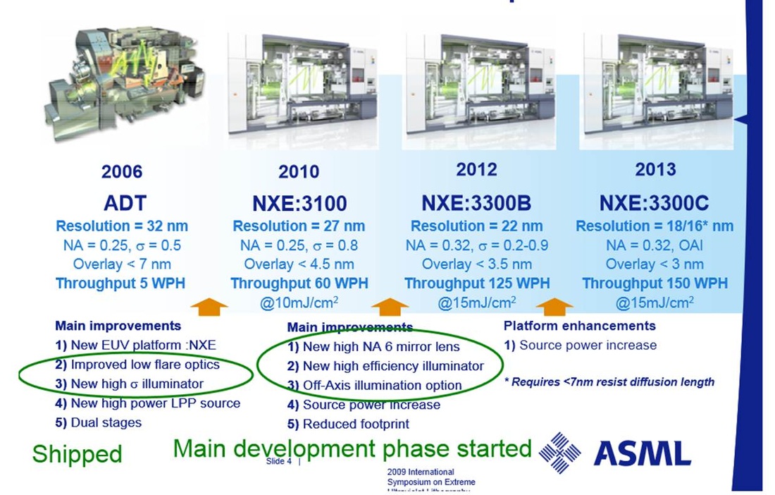
Figure 2: EUV road map
Picture
Figure 3: TSV road Map
It is not the purpose of this blog to go over the reasons why the roadmaps of EUV and TSV missed the time table by miles, nor to blame anybody for it. There are many articles and discussions published on the subjects. Rather, I will touch on some of the highlights as well as try to make some conclusions regarding the pathway of the industry regarding these two important technologies.

EUV: The EUV technology has so far gone through monumental achievements vis-à-vis the incredible tasks of developing the next generation stepper technology. The amount of engineering and resources poured into it is unprecedented in the short history of the semiconductor industry and maybe so for other industries.

It looks like as I write this blog that the only barrier for the technology from becoming a HVM tool is EUV source power that can provide a high enough throughput. Many experts doubt that it could ever be achieved; however, there are many other experts saying that it is within a reach.

TSV: In this case I could see two totally unrelated issues:

1. Technology driven obstacles

2. Logistics and supply chain issues.

In the case of the TSV it is one of the few cases where the "power point" presentation(s) of the TSV idea are so convincing that it is actually hard to oppose it. However, when it comes to the fine details of the technology development, there are many issues that still need to be addressed and resolved. I believe that it is just a matter of time before the technical obstacles will be resolved and a unified standardized solution emerges. However, on the other hand, I see a real problem from the point of view of logistics, cost and supply chain of the technology, and I have some doubts if it can ever be resolved. For further discussion on this issue, please refer to: 3D IC Supply Chain: Still Under Construction, and to a detailed comment in EE Time published blog and comments re. Semicon West 3D - IC TSV, provided here below.

In summary, I believe that the industry will come with a solution for EUV before TSV becomes a production technology.

Yet there is another alternative to TSV and to EUV - it is the Monolithic 3D methods. Moreover, it is very likely that monolithic 3D will reach volume production before EUV and TSV. As we already see the  NAND Flash vendors ramping up for production of 3D NAND.

The detailed comment fromm EE Times re. Semicon West 3D - IC  TSV:

PictureUSER RANK CEO
Re: Semicon Showed Support for 3D ICs  
chipmonk0   7/18/2013 1:46:13 PM

" same old same old ... " !! With such pollyannaish coverage, I am afraid that TSVs will remain the next hot interconnect tech even 5 years from now !

To provide a counter-point to all this happy talk, SemiCon had invited me to lead a 1 hr discussion at the Show on "Roadmap for TSVs and Alternatives from a Technology perspective ". Since Herb was not there, here are the key points :

1. unlike previous Advanced Packaging technologies like Flip Chip which we developed at IDMs like Motorola & Intel with both deep / broad expertise and product commitments, the development of TSVs has been going on mostly at overseas Govt. funded Laboratories in fits and starts and has then jumped to Foundries / OSATs. Xilinx' use of 2.5-d to integrate poorly yielding FPGAs has led to much irrational exuberance and then disappointment.

2. In the Winter of 2010 - 11 Samsung reported the first Wide I/O DRAM stack using TSVs. Great bandwidth even at 200 MHz & terrific power eff. But what the blogosphere neglected to report was that the yields were down in the mud and since then not much has been heard about Wide I/O from Samsung. Instead they keep bringing out conventional LP DDR at ever higher Clock Rates. JEDEC has actually postponed Wide I/O to 2015. 
3.  The development of TSV technology has been going on in Fabs who do not have to be sensitive to stress issues common in "thick film" type laminates / composites as is the case for filled vias. It is only now that they are waking up to it. Stress effects depend on the sq. of via dia., hence the new interest in shrinking them below 5 um. But integration & reliability problems ( at high Aspect Ratios both get worse ) have not been thought through. Moreover, Bonding stacked chips using the current method ( a sort of pidgin version of the technology I had invented nearly 20 years ago at Motorola for GaAs Power Amps that went into Cell Phones ) also introduces residual stress, affects electron mobility and shifts timing. 

4. While these slow-poke Govt. funded Euro Labs rediscover stress effects on device perf. and the perils of Cu metallurgy applied indiscriminately, there is at least one small Company outside Chicago that has already shifted to the non - obvious ( at least to these TSV-niks ) yet theoretically sound choice of using Tungsten ( a brittle and poor electrical conductor which can be compensated by Design but unlike Cu a close CTE match with Si ).

5. But thats not all Folks - this tiny Co. with just 3 PhDs and Physicists has also solved the biggest TSV integration problem thats keeping all these Labs and various Tool Vendors new to the game ( in Herb's Osterreich they love to build big complex "Maschine" - Physics be damned ) -- intent on optimizing their individual process steps ( e,g. back up wafer bond / debond ) at the risk of compromising the whole process -- awake at night.

6. We did cover more, e,g. as to how to get the electrical benefits of TSVs w/o actually having to drill holes in live Silicon, circuitry and packages that make it possible. We already have some of these Alternatives ( using the concept of Active Interconnects ) under development - especially for the very large Server & SmartPhone markets - and have started publishing.

7. TSV development is orders of magnitude more complex than Flip Chip and would benefit from the same type of brutal, theory-driven Program Management practiced at the world's largest semiconductor Co., but since they have money in the Bank to stay on Moore's Law and thus continue single chip solutions they don't need TSVs that badly. So unless there is a radical shake - up in the TSV programs "outside", incl. at the Foundries, the present slow pace of TSV development will persist.

Morale : give TSVs a fair chance, they need a respite from these overly enthusiastic bloggers, embarassingly out of their depth, and at Conferences lets not blather about Supply Chain Issues, the technical probems are not all solved yet
submit to reddit
1 Comment

The Future is the Interconnect: IITC

5/20/2012

1 Comment

 
Picture
We have a guest contribution today from Ze'ev Wurman, MonolithIC 3D Inc.'s Chief Software Architect. Ze'ev discusses the upcoming IITC and the contribution of 3D technology to minimizing wire-length distribution.

Does Size Matter?

The next International Interconnect Technology Conference (IITC 2012) will be held in San Jose in a couple of weeks (June 4-6). This is a good opportunity to recall that, in some sense, the reason for scaling silicon down has changed in recent years from packing more transistors in a square (or cubic) millimeter to increasing functionality and performance at reduced power. An ever higher fraction of the power dissipation resides in the interconnect – both in the net switching itself as well as in the ever-increasing number of repeaters required to re-power more and more “long” nets.

Estimates of the area dedicated to repeaters as technology shrinks vary but even if the early predictions of 70% cells being dedicated to repeaters at 32 nm may have not come to pass (Saxena, TCAD 2004), a large fraction of chip power is now dissipated by interconnect structures. This is particularly true in FPGAs where the interconnect share of routing-related dynamic power may easily reach 2/3 of the power, but even non-programmable devices have been reported to have half of their power dissipated in the wires already at 90nm. The following slide is from the 2006 High Performance Embedded Computing workshop.

Picture
Last year IITC included a paper from Georgia Tech (Dae Hyun Kim, et al., Impact of Through-Silicon-Via Scaling on the Wirelength Distribution of Current and Future 3D ICs) that explores the impact of 3D on the average wire-length of deep submicron ICs. This paper differs from many others in that it explores the impact as a function of TSV size, and it models TSVs from the currently feasible 5 micron, with a 5:1 aspect ratio for the corresponding 25 micron thick silicon layer, down to a futuristic 100 nm, with a 50:1 aspect ratio for a 5 micron thick layer. Such futuristic TSV actually gets close to a monolithic process, which can achieve silicon thickness of one micron and below. Here is a key chart from this paper:

Picture
As we can see, a small-sized TSV can significantly reduce the average wire-length by up to 50%, and reflects an improvement equivalent to two or three technology generations. In other words, a 4-way stacked 32nm chip with monolithic-style vertical connectivity can have wire-length distribution as good as a 16nm cutting edge technology, with the associated reduction in power and increase in performance, but using a relatively inexpensive and depreciated fab line.

Yet there is a fly in this ointment – TSVs with aspect ratio of 50:1 are not likely to happen, and using nanometer-TSV with extremely thin silicon layers to maintain AR below 10 creates problems of its own. Just recently IMEC reported stress issues at 25 micron thickness and “found that increase in the die thickness from 25 to 50 um resulted in a stress reduction of 3X. Final conclusions were that 50 um thickness die were currently much better option for scalable manufacturable process.” In other words, the road to nanometer-scale vertical connections does not go through scaling down TSVs but through monolithic process and layer transfer.

I find all this a nice illustration of the importance of the monolithic stacking approach that is also easily visible using our free simulator, IntSim.

Picture
Transformation to 3D monolithic stacking is much more than simply saving on a footprint by slicing and stacking the same design. The rich vertical connectivity offered by monolithic stacking significantly reduces the average distance between source and destination and therefore improves performance, saves power, saves total area, and allows players to continue using older process fabs to achieve cutting edge results at a cheaper cost. The chart below illustrates such savings at 22nm technology:
Picture
The future of Moore’s Law and the continued well-being of our industry is in the small nanometer-sized TSV, not in the big micron-sized TSVs used today that are so hard to manage. And let’s hope that the upcoming IITC will be at least as interesting as last year’s.

submit to reddit
1 Comment

Is TSV for real?

4/8/2012

0 Comments

 
Picture
We have a guest contribution today from Israel Beinglass, the CTO of MonolithIC 3D Inc. Israel discusses about TSVs. 

Have you read some of the recent TSV headlines?

1. January 31, 2012 - CEA-Leti launched a major new platform, Open 3D, that provides industrial and academic partners with a global offer of mature 3D packaging technologies for their advanced semiconductor products and research projects.

2. March 7, 2012 - Semiconductor fab equipment supplier Applied Materials Inc. (AMAT) opened the new Centre of Excellence in Advanced Packaging at Singapore's Science Park II with its partner in the endeavor, the Institute of Microelectronics (IME)

3. March 26, 2012 - PRNewswire - Semiconductor design/manufacturing software supplier Synopsys Inc. (Nasdaq: SNPS) is combining several products into a 3D-IC initiative for semiconductor designers moving to stacked-die silicon systems in 3D packaging.

It is amazing that after so many years of development and efforts and great presentations we are still not in a full production and still basic R&D as well as EDA still in infancy.

Most people in the Industry consider Merlin Smith and Emanuel Stern of IBM the inventors of TSV based on their patent “Methods of Making Thru-Connections in Semiconductor Wafers” filed on December 28, 1964 and granted on September 26, 1967, as shown below patent  number 3,343,256
Picture
Figure 1: IBM TSV patent
In April 12, 2007 IBM announced a breakthrough new 3D technology:
Armonk, NY - 12 Apr, 2007: IBM (NYSE: IBM) today announced a breakthrough chip-stacking technology in a manufacturing environment that paves the way for three-dimensional chips that will extend Moore’s Law beyond its expected limits. The technology – called “through-silicon vias” - allows different chip components to be packaged much closer together for faster, smaller, and lower-power systems… IBM is already running chips using the through-silicon via technology in its manufacturing line and will begin making sample chips using this method available to customers in the second half of 2007, with production in 2008.
Picture
Figure 2: Original story on TSV advantages followed IBM announcement
Figure 2 is taken from Ignatowski’s presentation made shortly after IBM’s TSV announcement. This type of argument where chip stacking is compared to 2 chips side by side has become the corner stone of the TSV story (http://www.sematech.org/meetings/archives/3d/8334/pres/Ignatowski.pdf).

Already at that point (2007) it was clear to IBM that there were many issues with the technology that needed to be resolved.  Figure 3 shows the IBM slide discussing some of the problems for implementing TSV for mass production.
Picture
Figure 3: Issues per IBM with the TSV technology
During the years following and through to today there have been many attempts to bring the technology to the mass production. All have been without real success. 
The professional literature is full of beautiful road maps showing how TSV is going to change the industry with “more than Moore” as the next scaling methodology. 
Figure 4 is the Advanced Packaging road map for Texas Instruments which is typical of most companies Packaging/TSV road maps.
Picture
Figure 4: TI Packaging Technology Trends Dec 2011
There are several issues that are facing the industry when trying to implement TSV technology: (not in any specific order)
Process issues:
  • Via etching and filling are extremely slow since the dimensions are very different from the “normal” dimensions the industry uses (single/multiple digit microns for depth and diameter vs. nanometers, plus aspect ratios>5)
  • Via, first, middle or last which way to go? Each affects the whole process logistics in differing ways
  • How to integrate wafers from different sources Logic from IDM and/or foundry and memory from a memory Fab
  • Wafer thinning, how to handle fully processed wafer 20-80 micron thick including bonding and de-bonding. Rumors are that both Applied Materials and TEL are developing this kind of a tool
  • Wafer-to-wafer (W2W) or die-to-wafer (D2W) bonding: each  have processing challenges
  • Singulation of the final product
  • Substrate (carrier)for TSV

Design and EDA:
  •  Design rules are currently not compatible with TSV
  •  Who is responsible for the “system” design if there are several sources for product to be integrated?
  • EDA is way, way behind
  • Thermal simulation and heat removal issues
Back end issues:
  • Foundries/IDM vs. OSAT, who is doing what and who picks up yield loss
  • Final test
  • Reliability
  • The major foundries have no memory knowledge or how to integrate the memory on top of logic
Cost:

            - Currently the cost associated with implementing TSV is at least for now higher than other solutions. This is hampering the motivation to develop and implement the TSV technology.

Also the CapEx to implement TSV needs to be addressed, Figure 5 is a table put together by ASE that shows the readiness of the various equipment needed to run a typical TSV process.
Picture
Figure 5: TSV equipment readiness per ASE
One of the key issues that some people are neglecting right now is the fact that we do have an interim solution to the problem. It may- probably not be the best solution and perhaps not the most elegant one but it does work. These are the variety of packaging techniques using chip on chip with wire bonding, and assortment solutions (PoP etc).
Picture
Figure 6: Alternative methods for 3D chip connectivity
The following are some of the comments made by industry experts over the last few months.

TSMC
Doug Yu’s keynote address at the 3D Architectures for Semiconductor Integration and Packaging Conference in December, he noted that TSMC intends to provide full 2.5F and 3D service including chip design and fabrication, stacking and packaging. Yu, who is senior director of integrated interconnect and packaging, R&D at TSMC, outlined the key technologies that offer the best path to commercializing 3D integration technologies, with the implication that TSMC is well positioned to provide them all.

(http://www.infoneedle.com/posting/100745?snc=20641)

“TSV is much more complex and challenging than ever before,” noted Yu. “There’s a new ballgame and a small window.” He said a conventional collaboration infrastructure is becoming harder. Integration must be simplified to reduce handling and an investment beyond conventional back-end (in other words, middle-end-of-line tools and processes) is required. In short, Yu said a full spectrum of expertise is needed that includes manufacturing excellence, capacity and customer relationships where there is no competition with the customer 


Hynix
Nick Kim VP of Packaging  announced that for Hynix, production of 3D devices is no longer a matter of if but when and how (http://www.infoneedle.com/posting/100669?snc=20641)

Kim provided a detailed cost breakdown illustrating why 3D TSV stacks are more expensive (1.3x more) than wire bond stacks to manufacture. Overall, TSVs alone add 25% to the manufacturing cost because there is additional cost at each step:  

  •  Design: net die area decreases due to TSV array. 
  •  Fab: increased process steps due to TSVG formation, and capex for TSV equipment. 
  •  Packaging: Bumping, stacking, low yield and CapEx for backside processing equipment such as temporary bond and de-bond. 
  • Test: Probe and final package test time is increased because of the need to test at each layer as well as final. 
  • Hynix 3D roadmap: volume TSV production will officially start after 2013:
  • DRAM on Logic for mobile applications in a known good stacked die (KGSD) driven by form factor and power, are in development in 2012 with low production expected early 2013 ramping to volume late 2014. 
  • DRAM on interposer in a 2.5D configuration for graphics applications, driven by bandwidth and capacity is in development in 2012 with low production expected by the end of the year and ramping to HVM early in 2014. 
  • 3D DRAM on substrate for high performance computing (HPC) driven by bandwidth and capacity is in development in 2012, with low production expected early 2013, ramping to volume late 2014. 

In terms of supply chain management, Kim sees Hynix favoring the open ecosystem where logic and memory prepared with/for TSV from foundries and IDMs going to OSATs for assembly.

Overall it looks almost like a nightmare to implement TSV in a manufacturing facility. Even if all the processes steps will be taken care of, the logistics and co-ordination with different Fabs and OSAT are definitely no fun!!!

It looks like when we sum all the issues regarding the TSV methodology for achieving 3D, the approach of monolithic 3D suggested by MonolithIC 3D could resolve many of these issues and offer a far greater cost/performance gain from going 3D. Most of these advantages were already discussed in previous blogs and are part of the company web site,

Just few items that I would like to highlight:
  •  Practically no limit on the amount of vias between the different chips in the stack.
  • No deep TSV – nanometers, not microns!
  •  All done within the IDM or the foundry – better yield control & ramp, and no pointing fingers.
Please comment and let’s get a discussion going.
submit to reddit
0 Comments

    Search Blog


    Meet the Bloggers


    Follow us


    To get email updates subscribe here:


    Recommended Links

    3D IC Community
    3D IC LinkedIn Discussion Group

    Recommended Blogs

    • 3D InCites by Francoise von Trapp
    • EDA360 Insider by Steve Leibson
    • Insights From the Leading Edge by Phil Garrou
    • SemiWiki by Daniel Nenni, Paul Mc Lellan, et al.

    Archives

    March 2022
    December 2021
    August 2021
    August 2018
    July 2018
    May 2018
    October 2017
    September 2017
    December 2016
    September 2016
    August 2016
    November 2015
    October 2015
    September 2015
    July 2015
    June 2015
    May 2015
    April 2015
    March 2015
    February 2015
    October 2014
    September 2014
    August 2014
    July 2014
    June 2014
    May 2014
    April 2014
    March 2014
    February 2014
    January 2014
    December 2013
    November 2013
    October 2013
    September 2013
    August 2013
    July 2013
    March 2013
    February 2013
    January 2013
    December 2012
    November 2012
    October 2012
    August 2012
    June 2012
    May 2012
    April 2012
    March 2012
    February 2012
    January 2012
    December 2011
    November 2011
    October 2011
    September 2011
    August 2011
    July 2011
    June 2011
    May 2011
    April 2011
    March 2011

    Categories

    All
    3d Design And Cad
    3dic
    3d Ic
    3d Nand
    3d Stacking
    3d Technology
    Brian Cronquist
    Dean Stevens
    Deepak Sekar
    Dram
    Education
    Heat Removal And Power Delivery
    Industry News
    Israel Beinglass
    Iulia Morariu
    Iulia Tomut
    Monolithic3d
    Monolithic 3d
    MonolithIC 3D Inc.
    Monolithic 3d Inc.
    Monolithic 3d Technology
    Moore Law
    Outsourcing
    Paul Lim
    Repair
    Sandisk
    Semiconductor
    Semiconductor Business
    Tsv
    Zeev Wurman
    Zvi Or Bach
    Zvi Or-Bach

    RSS Feed

© Copyright MonolithIC 3D Inc. , the Next-Generation 3D-IC Company, 2012 - All Rights Reserved, Patents Pending