
We have a guest contribution today from Israel Beinglass, the CTO of MonolithIC 3D Inc. Israel was an executive at Applied Materials for many years, and is considered one of the leading industry experts in epi technology. He served as a board member at SiGen in the late 1990s (for those who are not familiar with SiGen, it was one of the first companies that worked on ion-cut technology). In this post, Israel discusses and compares different techniques to obtain stacked monocrystalline semiconductor layers.
The idea of Monolithic 3D where several layers of devices are built, has been around for a few years. Many approaches were taken to create one or several layers of transistors on a completed first device (Transistor and interconnect).
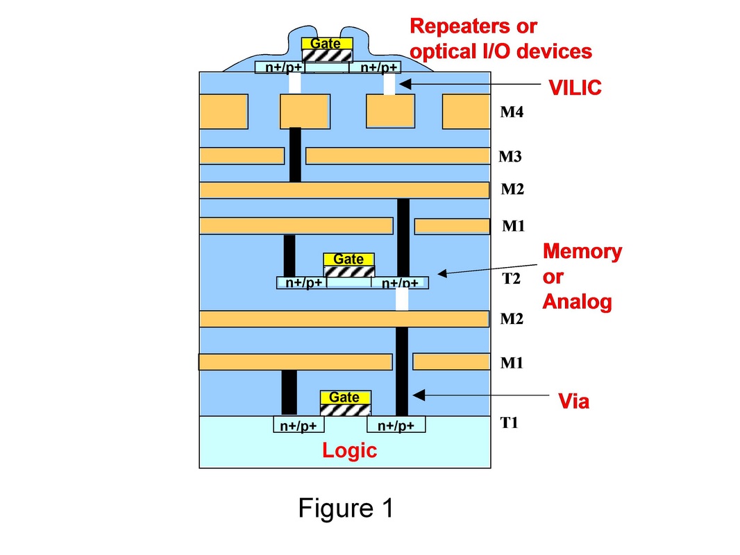
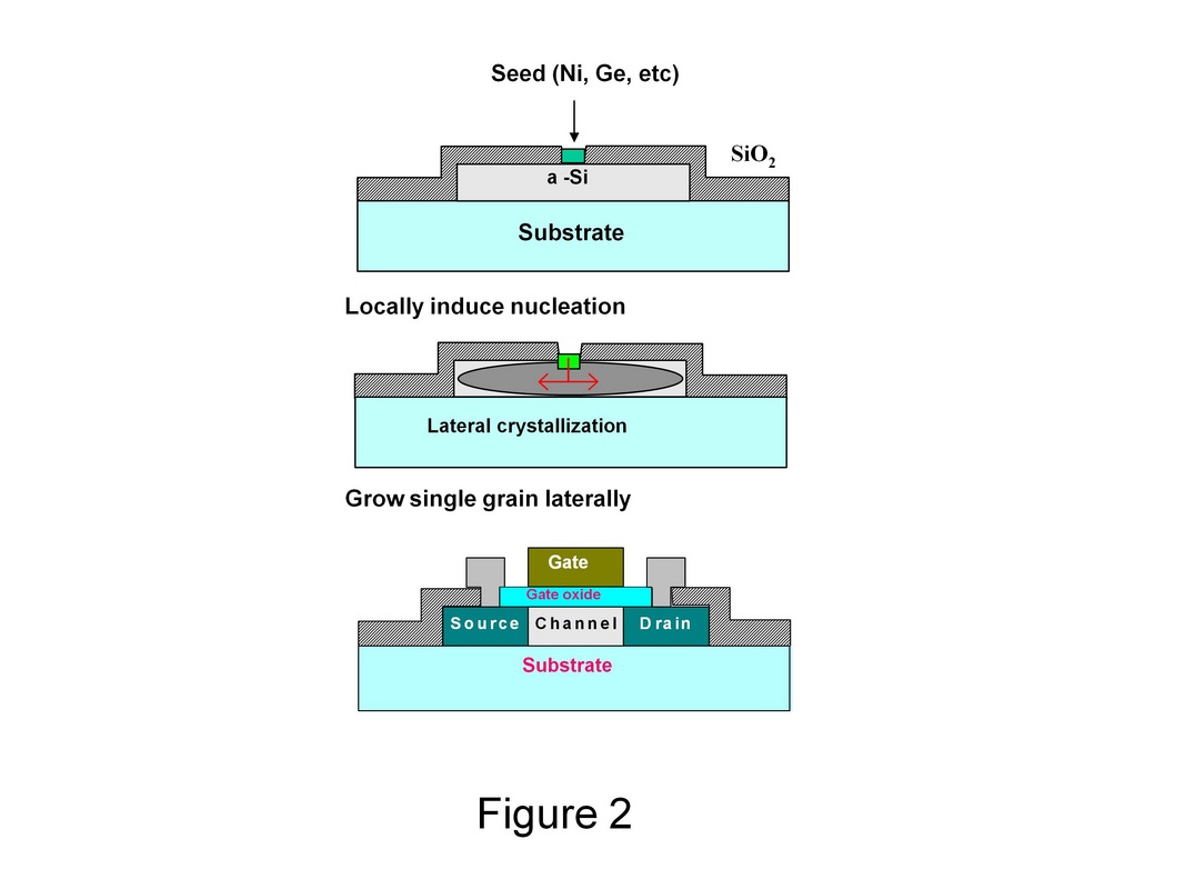
Saraswat in www.jbkempf.com/~jb/Post-CMOS/Stanford/Saraswat.ppt depicted the concept of multilayer Monolithic 3D with several “transistor levels” (Figure 1). Furthermore, he suggested to 1.nucleate and 2.crystallize amorphous silicon, forming the second level of transistors followed by another set of interconnect layers (Figure 2). Nucleating and crystallizing amorphous silicon turns to be a very difficult task especially when the chip has millions of transistors per level and when elevating the temperature could be detrimental. An alternative way is using TFTs on the second level of silicon, the problem with that is of course very poor performance of the transistors even after crystallization of the amorphous silicon to polycrystalline materials, as well as the need to generate S/D junctions at high temperature that will adversely affect the underlying devices.
Saraswat in www.jbkempf.com/~jb/Post-CMOS/Stanford/Saraswat.ppt depicted the concept of multilayer Monolithic 3D with several “transistor levels” (Figure 1). Furthermore, he suggested to 1.nucleate and 2.crystallize amorphous silicon, forming the second level of transistors followed by another set of interconnect layers (Figure 2). Nucleating and crystallizing amorphous silicon turns to be a very difficult task especially when the chip has millions of transistors per level and when elevating the temperature could be detrimental. An alternative way is using TFTs on the second level of silicon, the problem with that is of course very poor performance of the transistors even after crystallization of the amorphous silicon to polycrystalline materials, as well as the need to generate S/D junctions at high temperature that will adversely affect the underlying devices.
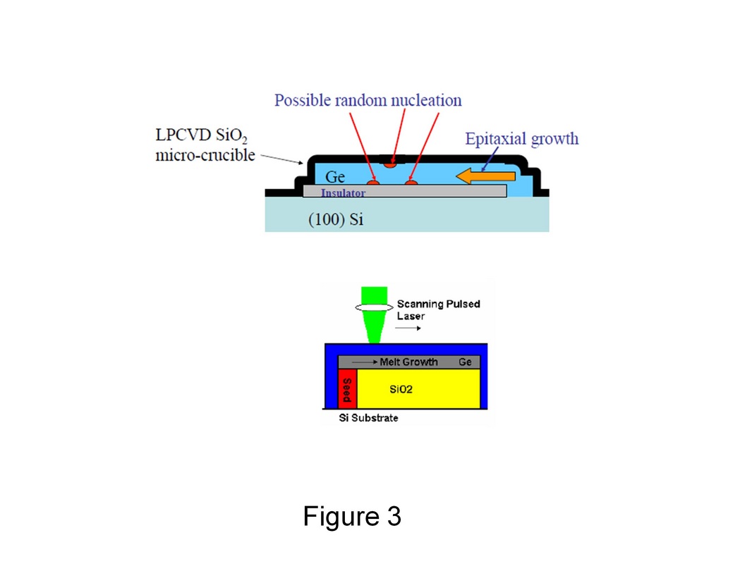
Another way which was suggested is low temperature Ge epitaxial over growth from “windows” in the silicon substrate and laser annealing the structure (Figure 3). This technology was developed by P. Griffin from Stanford and graduate students J. Feng, M. Kobayashi and G. Thareja (http://nanodevice.stanford.edu/3dworkshop/docs/8_Griffin-TEL3D-WorkshopNov07.pdf). They reported some limited success on growing epitaxial Ge. However fully integrating the technology seems to run into insurmountable difficulties of process control, as well as integrating Ge transistors on a full advanced CMOS process.
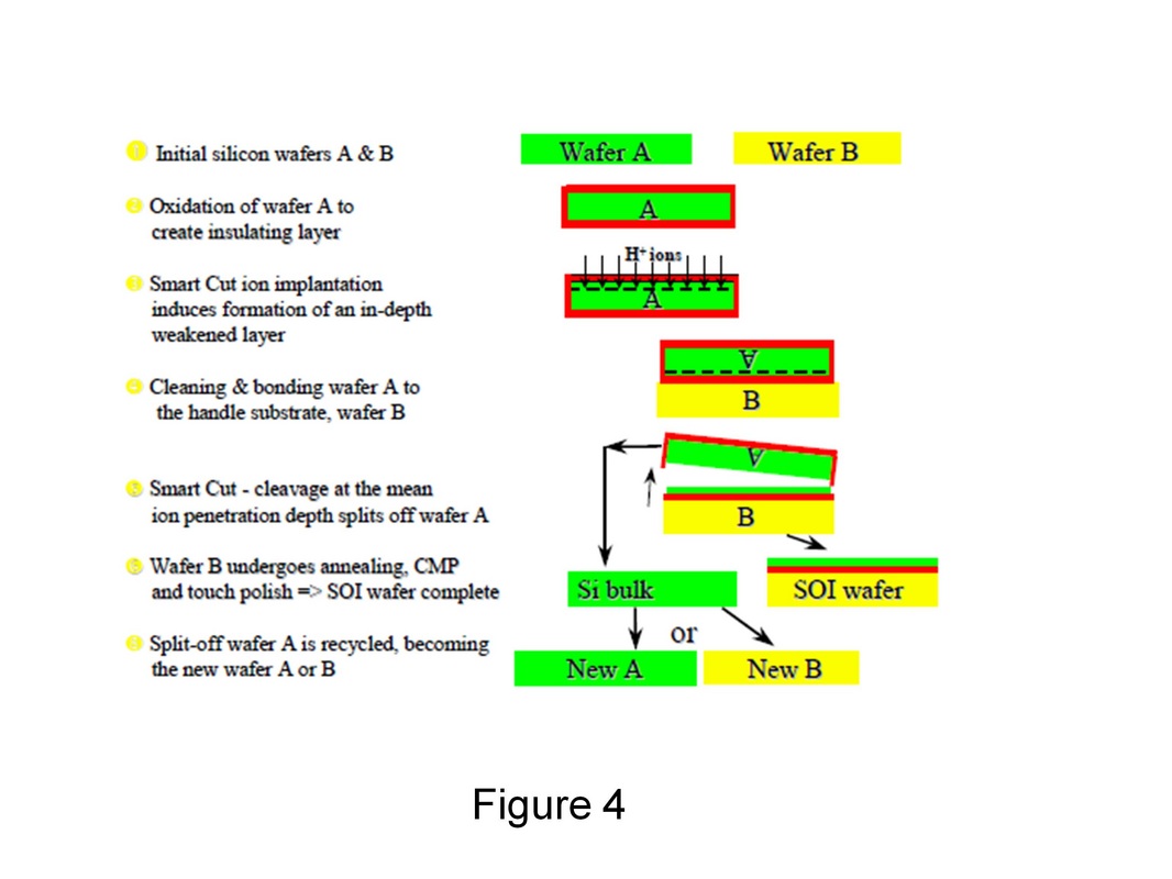
The other approach is integrating thin layer transfer onto a fully processed wafer, by that creating a second level of transistors, followed by a set of interconnect layers. The layer transfer is similar to the "smart-cut" process described by SOITEC in http://www.soitec.com/pdf/SmartCut_WP.pdf (Figure 4).
Applying layer transfer technology along with MonolithIC 3D Inc.’s IP portfolio is a new and fresh way to build the next generation of 3D device integration.


 RSS Feed