
We have a guest contribution from Zvi Or-Bach, the President and CEO of MonolithIC 3D Inc.
Starting as soon as 2016 Qualcomm is looking to leverage Monolithic 3D IC technology to win market share in the 8 billion smartphones that will be produced from 2014 to 2018 market, said Karim Arabi, vice president of engineering at Qualcomm, speaking at the International Symposium on Physical Design (ISPD-2015, Mar. 29-April 1). This was reported by the EE Times blog titled 3D Qualcomm SoC Testing on Horizon. Arabi’s presentation slides, along with the corresponding CEA Leti slides, are now available on the ISPD-2015 conference site.
Starting as soon as 2016 Qualcomm is looking to leverage Monolithic 3D IC technology to win market share in the 8 billion smartphones that will be produced from 2014 to 2018 market, said Karim Arabi, vice president of engineering at Qualcomm, speaking at the International Symposium on Physical Design (ISPD-2015, Mar. 29-April 1). This was reported by the EE Times blog titled 3D Qualcomm SoC Testing on Horizon. Arabi’s presentation slides, along with the corresponding CEA Leti slides, are now available on the ISPD-2015 conference site.
Qualcomm’s long term focus on Monolithic 3D was reviewed in our EE Times blog Qualcomm Calls for Monolithic 3D. Qualcomm calls it now “3DV” and plans to use it for future scaling. See the following slide presented by Arabi.
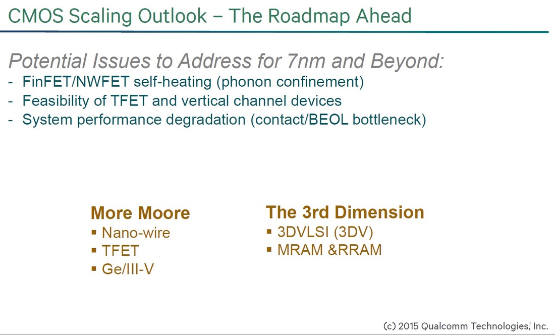
Figure 1
Quoting: "Our 3D VLSI technology, which we call 3DV, enables die size to be shrunk in half, while simultaneously increasing yields,”...“The final advantage of 3DV chips,” according to Arabi, “is that you only need to use the most expensive and latest node technology on the bottom layer. For instance, the bottom layer housing the CPU, GPU and other high-speed devices can be fabricated at 10-to-14 nanometer, whereas the higher layers housing less critical functions can be fabricated at a less expensive relaxed node of, say, 28-nanometers.”
The following slide presented by Arabi illustrates their Monolithic 3D technology (“3DV”) process flow, which seem very similar to the CEA Leti CoolCube program co-sponsored by Qualcomm.
The following slide presented by Arabi illustrates their Monolithic 3D technology (“3DV”) process flow, which seem very similar to the CEA Leti CoolCube program co-sponsored by Qualcomm.

In the fabrication process of front-to-back (F2B) 3DVs (a) the bottom tier is created the same way as 2D-ICs. (b,c,d) To add another layer, first a thin layer of silicon is deposited on top of the bottom tier. (e) This front-end-of-line (FEOL) process of the top tier permits the addition of normal vertical vias and top-tier contacts. (f) Finally back-end-of-line (BEOL) processing creates the top-tier. (Source:Qualcomm)
Arabi’s presentation also discussed the design tools available for Monolithic 3D. For the short term Qualcomm is planning to use conventional 2D EDA with scripts and an additional software program to design their Monolithic 3D devices as illustrated in the following two slides.
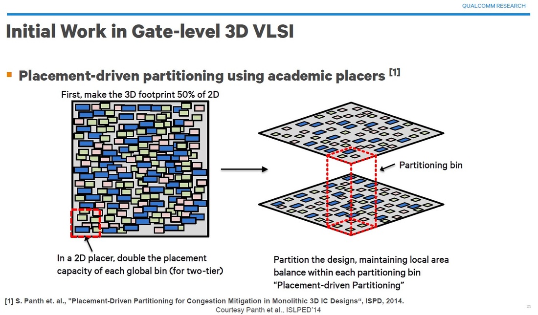
Figure 3
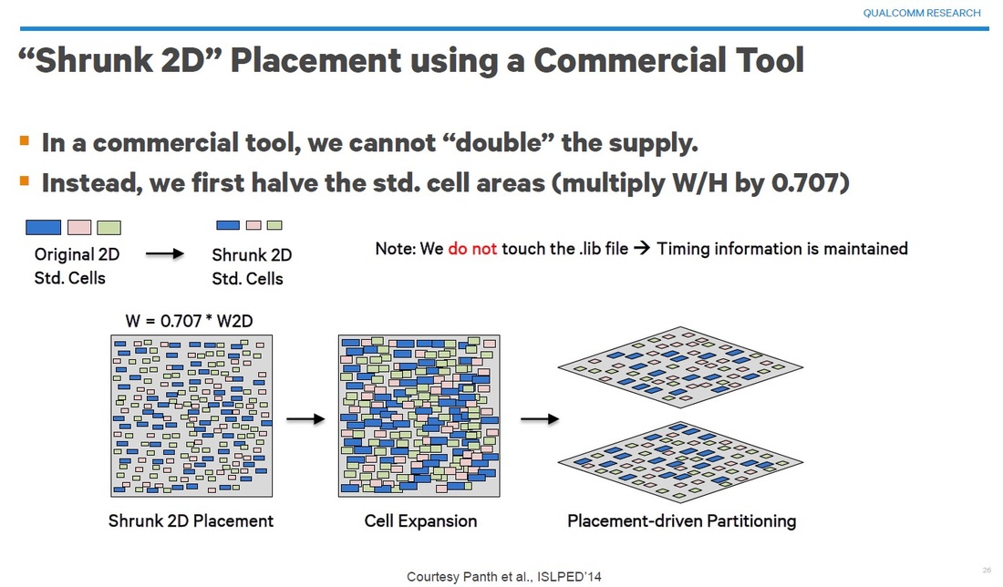
Figure 4
Arabi also discussed the Qualcomm work in respect to the thermal issues of such Monolithic 3D devices. The following summary slide provides the study’s conclusion: “3D temperatures are comparable or even better than 2D”.
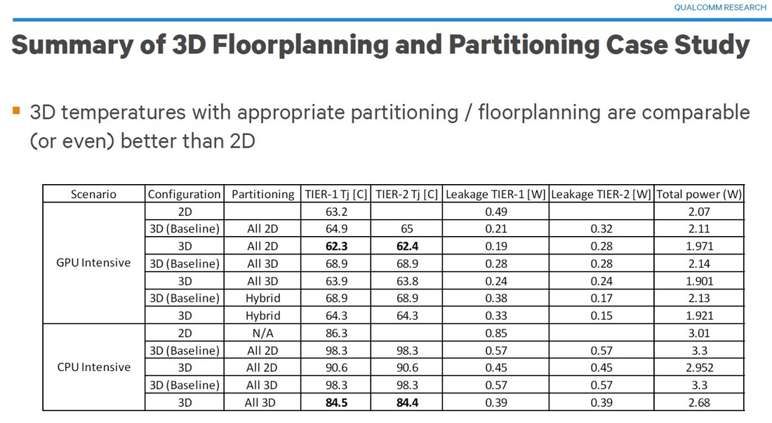
Figure 5
CEA Leti, Qualcomm’s technology partner, presented their joint work with Mentor Graphics on Monolithic 3D EDA. The following slide illustrates how Monolithic 3D could improve the on-chip interconnect challenge and why other forms of 3D IC, such as TSV, do not.
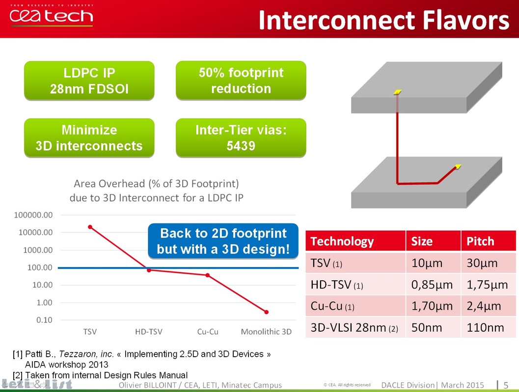
Figure 6
The following slide of CEA Leti presents the Qualcomm motivation for Monolithic 3D.

Figure 7
Quoting from a Cadence blog titled: Moore’s Law 2.0—The End and Beginning of a New Era! – “At the sub-10nm level, electromigration, and process variations in manufacturing, amongst other effects, will be so large that the end of conventional silicon chip manufacturing at high yields and chip longevity might be reached. However, we have a way out of this predicament. The solution is to build up. If we cannot make it 2D anymore, let’s make it 3D. Think about Manhattan, in New York City. When 2D space gets tight you build up into 3D space. The same thing is occurring in semiconductor manufacturing.”
The memory industry is ramping up Monolithic 3D as we speak. 3D NAND has seen announcements from Intel, Micron and Toshiba joining Samsung. Now the logic industry is looking to adopt Monolithic 3D as we learn from this Qualcomm presentation at this ISPD-2015 and the Intel presentation at ISSCC-2015 discussed in our recent blog Intel Call’s for Monolithic 3D.
P.S.
A good conference to learn about this new scaling technology is the IEEE S3S ‘15, in Sonoma, CA, on October 5th thru 8th, 2015. CEA Leti is scheduled to give an update on their CoolCube program and three leading researchers from Berkeley, Stanford and Taiwan’s NLA Lab will present their work on advanced monolithic 3D integration technologies.


 RSS Feed