Antifuse-based 3D High Density FPGA
Follow links for presentation on: 3D FPGA and Derivitive 3D FPGA.
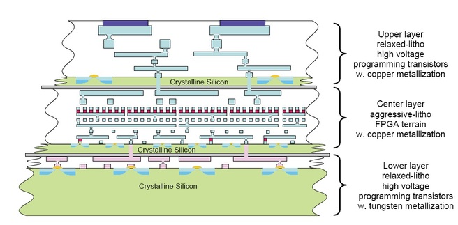
Antifuse-based 3D High Density FPGA
Technology
|
Benefits
|
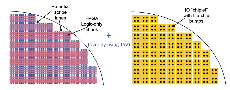
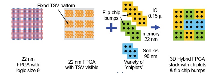
Inexpensive Arbitrary‐sized FPGA Manufacturing Fab
Assembly
Technology
|
Benefits
|