Monolithic 3D Inc., the Next Generation 3D-IC Company
  • Home
  • Technology
    • Technology
    • Papers, Presentations and Patents
    • Overview >
      • Background
      • Why Monolithic 3D?
      • Paths to Monolithic 3D
      • Applications
    • Ion-Cut: The Building Block
    • Monolithic 3D Logic >
      • RCAT
      • HKMG
      • Laser Annealing
      • RCJLT
      • 3D Embedded RAM
      • 3D Gate Array
      • FPGA
      • Ultra Large Integration - Redundancy and Repair
    • Monolithic 3D Memory >
      • 3D DRAM
      • 3D Resistive Memories
      • 3D Flash
    • Monolithic 3D Electro-Optics >
      • 3D Image Sensors
      • 3D Micro-Displays
  • 3D-IC Edge
    • 3D-IC Edge
  • News & Events
    • News & Events
    • S3S15 Game Change 2.0 Video/P
    • Webcast
    • Webinar
    • Press Releases
    • In the News
    • Upcoming Events
  • About Us
    • About Us
    • History
    • Team
    • Careers
    • Contact Us
  • Blog
  • Simulators

Semiconductor Equipment Manufacturing - Who wins from the recent consolidation

2/27/2012

3 Comments

 
Picture
We have a guest contribution today from Israel Beinglass, the CTO of MonolithIC 3D Inc. Israel discusses about the semiconductor equipment manufacturing: "Who wins from the recent consolidation?"

2011 was a big year for consolidation in the semiconductor equipment manufacturing industry. The year started with the Varian acquisition by Applied Materials and was ended with the merger announcement of Novellus and Lam Research (not concluded when this blog is written).

The equipment business is relatively conservative and for many years only few noticeable successful M&A were done. Few past M&A were of a strategic nature. In these cases a large corporation buys a smaller one to either develop a product line or to buy into a growing product line. Table 1 is a snapshot of some past M&A activities in the short history of the semiconductor equipment industry-by far not a complete list.
Picture
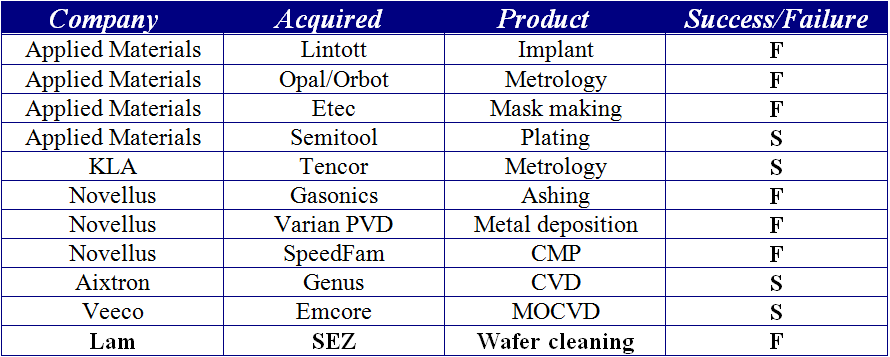
Table 1 - Past M&A activities
As one can see many of the M&A turned to be a failure and became a big drain on the acquirer balance sheet. In several cases the company seized operation of the acquired company after several years, in other cases it is still going on with a moderate or very limited success. To mention two cases of a real success I can point to the Veeco acquisition of the MOCVD from Emcore and the merger of KLA with Tencor. In both cases the M&A dramatically boosted the company’s position, market cap and market share.

Going back to the two recent M&A namely Applied Materials Varian and Lam Novellus the question is how this will affect the semiconductor industry and who is going to benefit from it.

I definitely view these two activities in a positive way.

1.   Applied Materials and Varian: Looks like Varian had practically all the implant market and really didn’t have any room to grow (beside the new solar implant business-highly speculative). So selling the company to Applied Materials helped a lot… the employees and the top executives that suddenly got their stock price almost double…From Applied Materials point of view they now controlling most of the front end equipment and can influence the transistor technology more than before. Though I might emphasize as I mentioned in a previous Blog that the percentage of the implant business in the whole semi CapEx pie is shrinking in the last few years and probably with the introduction of the FINFET-Tri gate it will shrink even more. Still for Applied strong position in the Epi, RTP and Implant market they do have good position in the front end. The missing link of course is a good position in the ALD technology (controlled by ASMI).

In other hand customers don’t like to see too much power at the hand of one equipment vendor; they do like to see competition. Not clear how it will be played in the implant arena since no other real competitor in the horizon.

2.   LAM Novellus: This merger was proposed many years ago and almost every year was rumored to go through without actually happening to the dismay of analysts and others. However eventually it did happen! By combining the winning position of Lam in the etch and Novellus in the CVD the new combined company could expand and offers new modules and combinations of products especially in the back end and in the emerging double (quadruple) patterning that becomes a very important module in the advanced lithography.

In order to complete this discussion we need to look at the future, and in the future new technology of 3D devices will become a reality. Let’s discuss now how these M&A will affect the new world of 3D devices.

  1. TSV
    1. No real effect from the Applied Materials Varian deal since the implant is only a front end technology. Not clear if the Plasma Doping (PLAD) that supposes to do material modifications has any impact in the back end.
    2. For the Lam Novellus deal it could enhance the TSV technology since they could bring a more comprehensive solution to the TSV module that will include the etching, deposition and Cu plating. Of course they are missing the market leading position that Applied Materials has in the Cu barrier seed PVD equipment.
  2. Monolithic 3D
    1. Since Applied Materials own now the implant business they could easily get involved in the smart cut technology from point of view of proliferate it to the rest of the world, as it is currently dominate only by the SOI wafers manufacturing. Owning the RTP and Epi helps well in the Monolithic 3D module.
    2. No real effect from the Lam Novellus deal.
    3. The future introduction of Monolithic 3D technology into the Fab present an opportunity to all the equipment manufacturing companies from several new tools that need to be proliferate into the process flow.
submit to reddit
3 Comments

Why Samsung will give Morris Chang sleepless nights

2/5/2012

13 Comments

 
Samsung contributes just 7% to the world’s foundry revenue today. But here’s why it could be TSMC’s biggest challenge yet...

Most people will agree that Andy Grove has been the semiconductor industry's most successful CEO. After co-founding Intel and serving as COO for many years, he took over the CEO role and oversaw a 2400% increase in the company’s stock price. Among the present set of semiconductor CEOs, does anyone possess Grove’s high levels of performance, dynamism and vision? There can be only one answer: Morris Chang, the founder and CEO of TSMC.

I’m sure many of you have read Andy Grove’s classic book, “Only the Paranoid Survive”. Let’s now apply the principles in Grove’s book to the foundry industry. If you were Morris Chang and had 50% market share in the foundry industry, which competitor of yours would you be “paranoid” about?

Picture
Figure 1: Foundry Revenue in 2011 (Source: SemiMD).

Fig. 1 shows the foundry landscape at the end of 2011. Many competitors show up: there’s Globalfoundries with its plentiful oil money, UMC with its excellent customer service and high yields and SMIC with its Chinese government backing. But, to me, Samsung is undoubtedly the biggest threat to TSMC, even though its foundry market share today is just 7%. Let me explain why...

Economies of Scale due to Memory Business

Semiconductor manufacturing costs are heavily dependent on economies of scale. Fig. 2 [1][2], which is an estimate of DRAM costs and selling prices in 2003, illustrates this point. The highest volume producer, Samsung, has the lowest raw material costs in Fig. 2. The same goes for semiconductor equipment purchases. A higher volume producer gets a lower price per tool. You’ll notice the highest volume producer (Samsung) has the lowest depreciation cost in Fig. 2.
Picture
Figure 2: DRAM industry landscape in 2003. Costs are a function of production volumes. (Source: [1][2])

What does this mean for the foundry industry? Well, TSMC, since it has 50% market share, should benefit from economies of scale and build a lead over its rivals, right? That certainly gives TSMC an advantage over UMC and Globalfoundries, but doesn’t work with Samsung. Why? Because Samsung owns a huge chunk of the world’s memory business (~40%). It buys tools and raw materials in huge volumes for those markets, and you use pretty similar tools and raw materials for logic foundry manufacturing. Fig. 3 illustrates that Samsung’s capital expenditure for tools in 2012 is actually double that of TSMC. Samsung might therefore have lower raw material costs and depreciation costs than TSMC.

Picture
Figure 3: Samsung buys more semiconductor equipment than TSMC (numbers shown for 2012). Scale of equipment buying provides low prices. (Source: SemiMD)

Yield improvement methodologies

Samsung has a great set of yield improvement methodologies developed over its years in the competitive memory industry. Fig. 5 [2] illustrates yields of different DRAM manufacturers in 2003. You’ll notice Samsung has, by far, the best yields. Based on this data and Samsung’s reputation for high-yield memory products, you would expect Samsung to get good yields in the logic foundry business.  They seem to be delivering on that front. I hear from industry contacts that Samsung is the only manufacturer getting reasonable yields for gate-first high k metal gate products at 28nm.
Picture
Figure 4: Samsung’s yield enhancement methodologies gave it an advantage over competitors in the memory industry. (Source: [2])

Low cost fabs

In cost sensitive markets such as memory and foundries, the location of a fab makes a difference. Fig. 5 [3] shows a chart from the US National Academy of Engineering which reveals that fab costs in the US are ~25% higher than fab costs in the Far East. Some of TSMC’s competitors have fabs in Europe and the US, but Samsung is building a good portion of its capacity in Korea (they do have one facility in Texas though). The fab cost advantage TSMC has over its other competitors doesn’t necessarily exist with Samsung.
Picture
Figure 5: Cost of US fabs higher than those in Korea, Taiwan or Singapore. (Source: [3])

Sensible partnership strategy

One of the barriers to entry for the foundry business is availability of Intellectual property (IP) blocks and CAD tool support. Intel, which is looking to enter the foundry business, has difficulties with this, since IP blocks haven’t been developed for its technologies yet. SoC makers today show a marked preference for foundries offering competitive IP blocks at low prices.

When Samsung entered the foundry industry, it addressed this issue by joining the IBM alliance, and so its customers could use IP blocks developed for the IBM alliance. Samsung did not have much experience developing logic technologies either, and the alliance helped Samsung learn from existing players in the logic business such as IBM and Globalfoundries. In spite of having a similar technology offering to Globalfoundries and IBM, Samsung retains an advantage over these competitors since it is better at ramping up yields and because it has low cost fabs.

R&D costs for next-generation logic technologies are $1-2 billion today. Sharing the cost with IBM and Globalfoundries gives Samsung a R&D cost advantage over companies such as TSMC and UMC which develop new technologies alone.

Ability to fund large capital expenditures

TSMC, UMC, Globalfoundries and SMIC derive almost all their sales from the foundry industry. This limits the amount of capacity they can add every year, since their balance sheets place restrictions on maximum cap-ex to revenue ratio (Globalfoundries is an exception here due to its oil money). Samsung, on the other hand, is a diversified company that sells everything from TVs to DRAM to NAND flash to cell phones. It routinely takes profits from other divisions and invests it in the logic foundry industry. Fig. 6 [4] illustrates this trend. Samsung’s capex to revenue ratio for its foundry business is way higher than anyone else. This added capacity is helping Samsung’s foundry business grow rapidly  – notice how Samsung’s froundry revenues increased almost 7x between 2010 and 2012. Samsung used this “capacity-add-like-there-is-no-tomorrow” strategy to become our industry’s biggest DRAM producer, so the foundry folks had better watch out!
Picture
 Figure 6: Samsung has the highest cap-ex to revenue ratio among all foundries. (Source: SemiMD)

Proven Research Expertise

If you talk with engineering folks in our industry and ask them which companies do the best research, you will find Samsung near the top of the list. Let me illustrate Samsung’s research capabilities using Monolithic 3D as an example. They started working on the technology almost 10 years back, and have developed monolithic 3D technologies for NAND flash, SRAM and resistive memories. In addition, their roadmap calls for commercialization of Monolithic 3D NAND flash memories within 2 years. Check out Fig. 7. This is some of the best work I’ve seen on monolithic 3D so far. This phenomenal research capability will help Samsung make strides in the logic space.
Picture
Figure 7: Samsung has a long history of developing monolithic 3D technologies.

Caveat

While the above capabilities of Samsung threaten TSMC in the long term, there are stormy clouds looming for Samsung in the short term. Apple, which accounts for more than 75% of Samsung’s foundry revenues [4] today, is flirting with TSMC due to its increasingly litigious competition with Samsung in the mobile space. If TSMC executes well and takes this business away from Samsung, it could be a big blow to Samsung’s ambitions.

To summarize

I explained why I believe Morris Chang will consider Samsung his biggest competitor in the long-term. The economies of scale Samsung has due to its memory business could help its logic operations. Samsung’s superb yield ramp capabilities and low cost Korean fabs are another key asset. Probably the biggest weapon Samsung has is its conglomerate (chaebol) structure, which allows it to make huge capital investments and grow rapidly.

At the start of this write-up, I talked about how Morris Chang has grown TSMC the way Andy Grove grew Intel. One of Andy Grove’s strengths was that he recognized Intel’s biggest challenges, and channelized his “paranoia” and limitless energy into finding counter-measures. What can Morris Chang do to deal with “the Samsung challenge”? In a future blog post, I will describe strategies for this... stay tuned!

- Post by Deepak Sekar

submit to reddit
13 Comments

    Search Blog


    Meet the Bloggers


    Follow us


    To get email updates subscribe here:


    Recommended Links

    3D IC Community
    3D IC LinkedIn Discussion Group

    Recommended Blogs

    • 3D InCites by Francoise von Trapp
    • EDA360 Insider by Steve Leibson
    • Insights From the Leading Edge by Phil Garrou
    • SemiWiki by Daniel Nenni, Paul Mc Lellan, et al.

    Archives

    March 2022
    December 2021
    August 2021
    August 2018
    July 2018
    May 2018
    October 2017
    September 2017
    December 2016
    September 2016
    August 2016
    November 2015
    October 2015
    September 2015
    July 2015
    June 2015
    May 2015
    April 2015
    March 2015
    February 2015
    October 2014
    September 2014
    August 2014
    July 2014
    June 2014
    May 2014
    April 2014
    March 2014
    February 2014
    January 2014
    December 2013
    November 2013
    October 2013
    September 2013
    August 2013
    July 2013
    March 2013
    February 2013
    January 2013
    December 2012
    November 2012
    October 2012
    August 2012
    June 2012
    May 2012
    April 2012
    March 2012
    February 2012
    January 2012
    December 2011
    November 2011
    October 2011
    September 2011
    August 2011
    July 2011
    June 2011
    May 2011
    April 2011
    March 2011

    Categories

    All
    3d Design And Cad
    3dic
    3d Ic
    3d Nand
    3d Stacking
    3d Technology
    Brian Cronquist
    Dean Stevens
    Deepak Sekar
    Dram
    Education
    Heat Removal And Power Delivery
    Industry News
    Israel Beinglass
    Iulia Morariu
    Iulia Tomut
    Monolithic3d
    Monolithic 3d
    MonolithIC 3D Inc.
    Monolithic 3d Inc.
    Monolithic 3d Technology
    Moore Law
    Outsourcing
    Paul Lim
    Repair
    Sandisk
    Semiconductor
    Semiconductor Business
    Tsv
    Zeev Wurman
    Zvi Or Bach
    Zvi Or-Bach

    RSS Feed

© Copyright MonolithIC 3D Inc. , the Next-Generation 3D-IC Company, 2012 - All Rights Reserved, Patents Pending