Monolithic 3D NAND Flash Memories
Technology
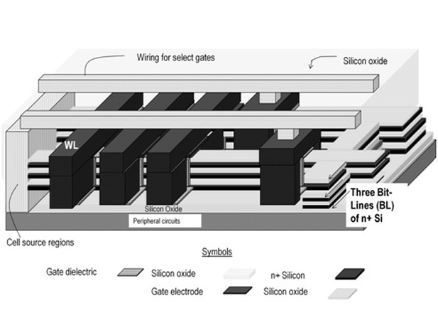
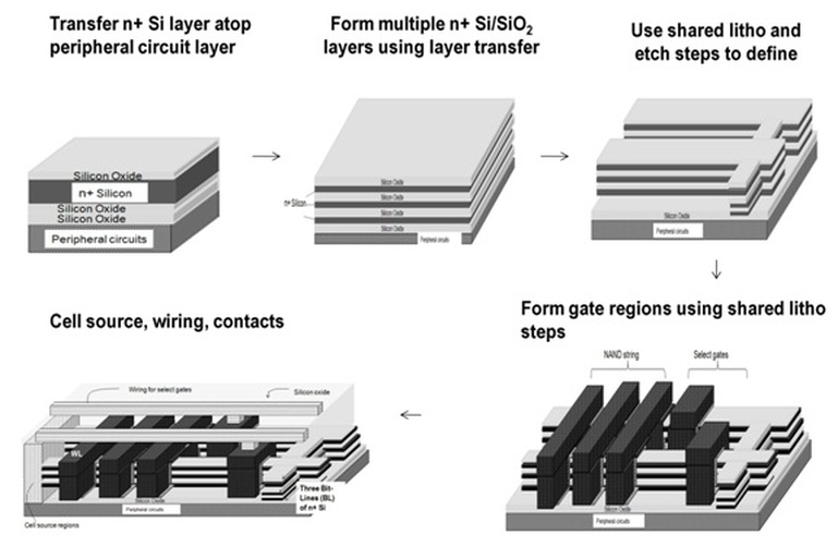
Monolithic 3D IC technology is applied to producing a monolithically stacked single crystal silicon double-gated NAND flash memory. Lithography steps are shared among multiple memory layers to reduce bit cost. Peripheral circuits below the monolithic memory stack provide control functions.
Reduce NAND flash bit cost without investing in expensive scaling down. |
Benefits
|
Process Flow
Our 3D flash technology innovatively combines these well-studied technologies:
- Monolithic 3D with litho steps shared among multiple memory layers
- Stacked Single crystal Si with ion-cut
For more details, please see
[1] Our blog post titled "Looking beyond lithography", April 2011.
[2] Our blog-post on cost of ion-cut, July 2011.
[2] Our blog-post on cost of ion-cut, July 2011.


