"The Evolution of Scaling from the Homogenous Era to the Heterogeneous Era"

We have a guest contribution from Zvi Or-Bach, the President and CEO of MonolithIC 3D Inc. Zvi underlines the milestone for monolithic 3D in the semiconductor road map 2019.
In the recent CEA Leti day, that took place as part of Semicon West 2013, Laurent Malier, Leti CEO presented his "A look at the coming Decade".
Slide 15 of the presentation provides Leti vision for CMOS roadmaps as presented here:
Slide 15 of the presentation provides Leti vision for CMOS roadmaps as presented here:
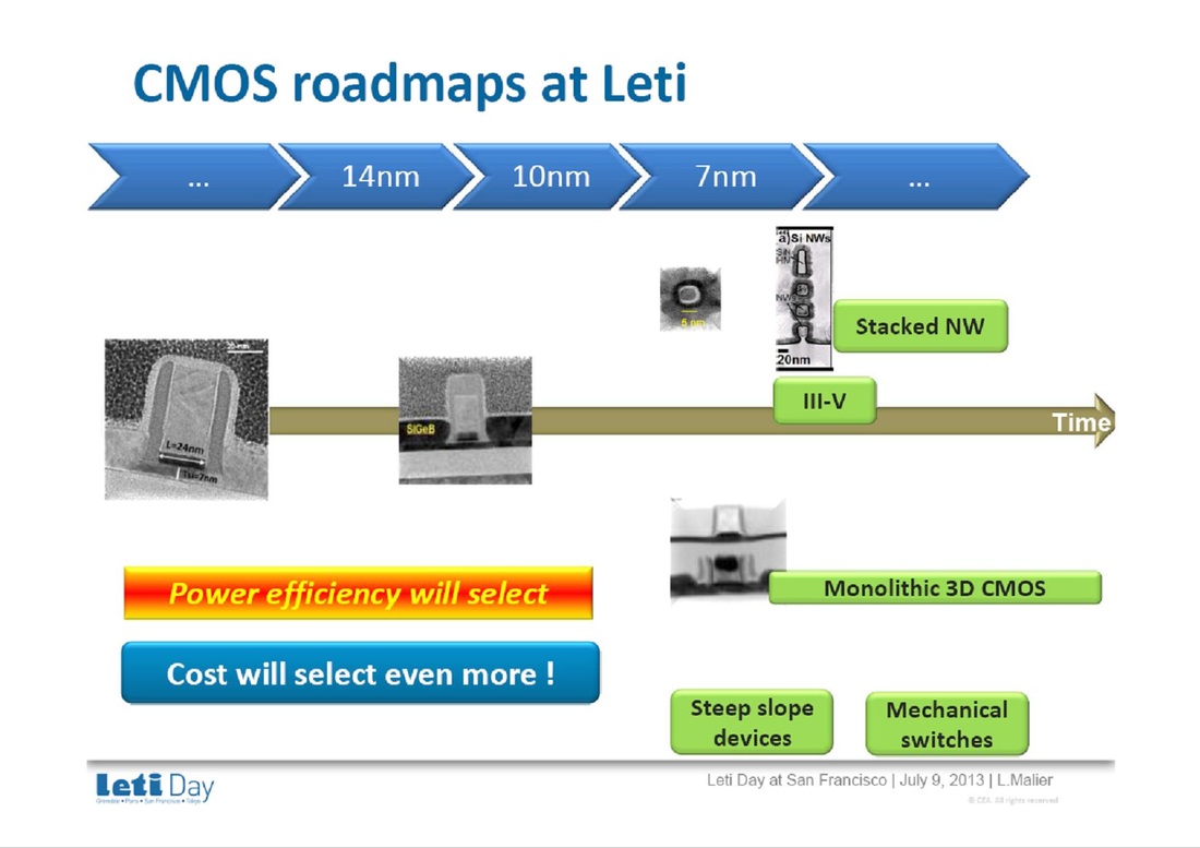
Figure 1
Monolithic 3D is presented on the road-map as the technology to follow 7nm process node.
Early this year we blogged - IEDM 2012: The pivotal point for monolithic 3D ICs, it is quite reassuring to see monolithic 3D now as part of the industry road-map. As we discussed than the memory vendors are already gearing up for volume production of the 3D NAND as reported recently Toshiba to Build Fab for 3D NAND Flash, leveraging monolithic 3D cost reduction advantage. It only makes senses for the CMOS market to follow. Doubters would ask why the industry would introduce new dimension to a road map that has been extremely successful for over 40 years. And the answer is very simple - because it is successful any more. We are all aware that the escalating costs of lithography had diminished transistors cost reduction as illustrated in the following ASML chart
Early this year we blogged - IEDM 2012: The pivotal point for monolithic 3D ICs, it is quite reassuring to see monolithic 3D now as part of the industry road-map. As we discussed than the memory vendors are already gearing up for volume production of the 3D NAND as reported recently Toshiba to Build Fab for 3D NAND Flash, leveraging monolithic 3D cost reduction advantage. It only makes senses for the CMOS market to follow. Doubters would ask why the industry would introduce new dimension to a road map that has been extremely successful for over 40 years. And the answer is very simple - because it is successful any more. We are all aware that the escalating costs of lithography had diminished transistors cost reduction as illustrated in the following ASML chart
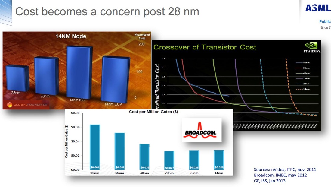
Figure 2
But even if we ignore these issues we should remember that "Atoms don't scale" (as was phrased by Bernie Meyerson of IBM), and we are quickly approaching these limit as is presented by the following Intel chart:
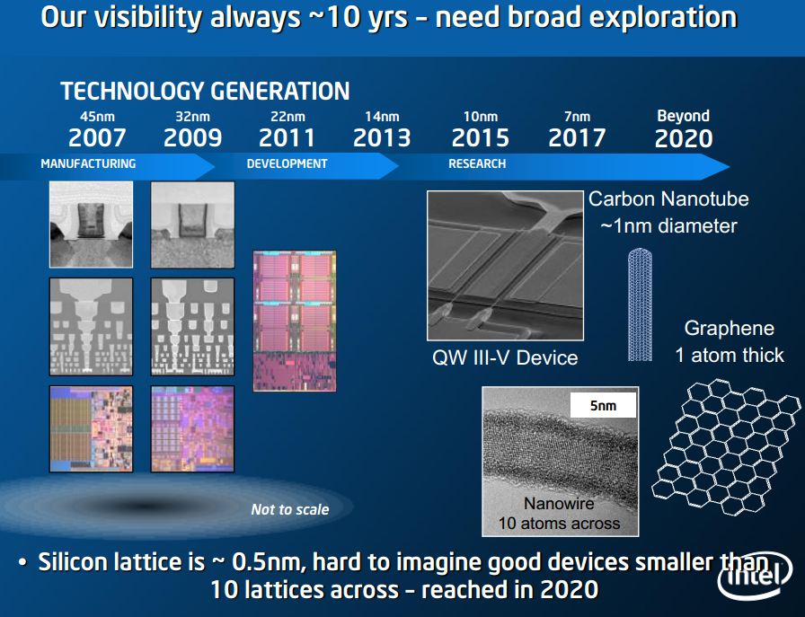
Figure 3
And accordingly Mike Mayberry, director of its component research at Intel, said at the very recent IMEC Technology Forum "...has looked down the highway of conventional silicon development and reckons things become foggy beyond about the 7-nm node".
In fact Mike in his March 2013 presentation titled "Pushing Past the frontiers of Technology" clearly also present the monolithic 3D on his road map as the following slides illustrates
In fact Mike in his March 2013 presentation titled "Pushing Past the frontiers of Technology" clearly also present the monolithic 3D on his road map as the following slides illustrates
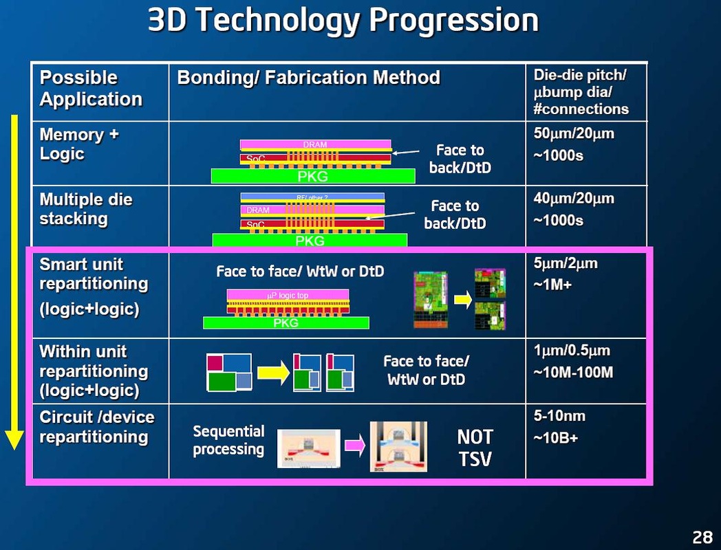
Figure 4
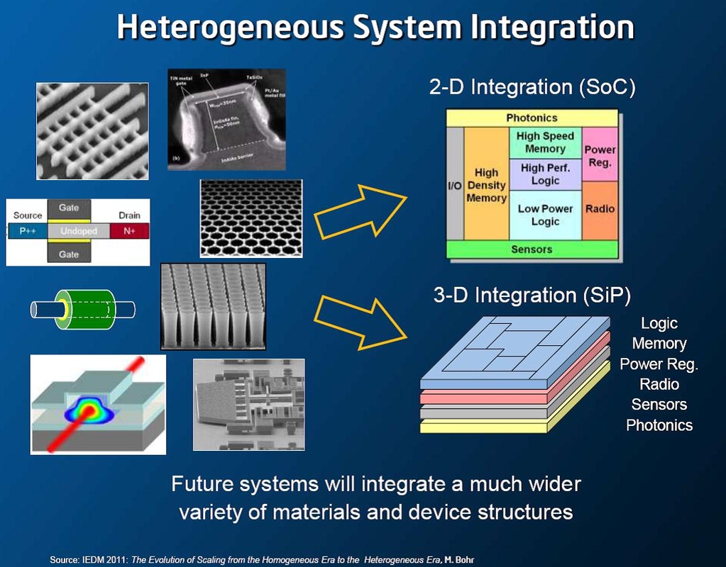
Figure 5
As was very well stated by Mark Bohr - Senior Fellow of Technology and Manufacturing Group and a Director of Process Architecture and Integration of Intel:
"The Evolution of Scaling from the Homogenous Era to the Heterogeneous Era"


 RSS Feed