
"For the past 40 years, conventional flash memory has been based on planar structures that make use of floating gates. As manufacturing process technology has proceeded to the 10nm-class and beyond, concern for a scaling limit arose, due to the cell-to-cell interference that causes a trade-off in the reliability of NAND flash products. This also led to added development time and costs.
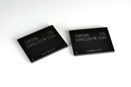
Samsung's new V-NAND solves such technical challenges by achieving new levels of innovation in circuits, structure and the manufacturing process through which a vertical stacking of planar cell layers for a new 3D structure has been successfully develop...
Also, one of the most important technological achievements of the new Samsung V-NAND is that the company's proprietary vertical interconnect process technology can stack as many as 24 cell layers vertically, using special etching technology that connects the layers electronically by punching holes from the highest layer to the bottom. With the new vertical structure, Samsung can enable higher density NAND flash memory products by increasing the 3D cell layers without having to continue planar scaling, which has become incredibly difficult to achieve”
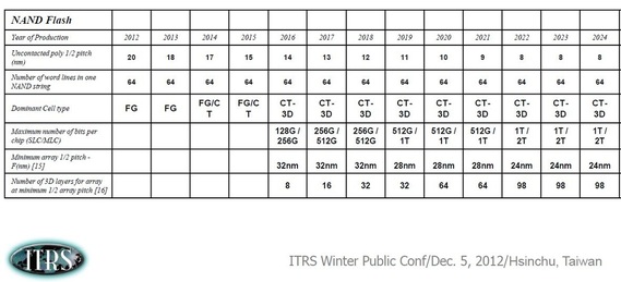
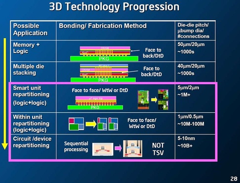
It’s worth mentioning to the point that while the volume production of TSV based 3D IC is keep being pushed out as discussed in a recent blog: EUV vs TSV: Which one will become production ready first?, this announcement indicates that monolithic 3D NAND is biting the forecast by few years as being illustrated by the following 2012 ITRS chart:
Monolithic 3D technology provides multiple unique and powerful advantages as we present on our site under the tab: 3D-IC Edge. Under item 5 we present the unique advantage that was first introduced in 2007, when Toshiba unveiled its Bit Cost Scalable (BiCS) technology. The unique advantage of 3D NAND is the ability to pattern and process multiple layers simultaneously.
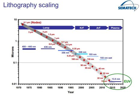
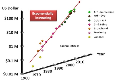
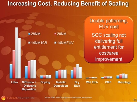
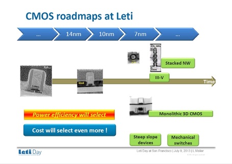
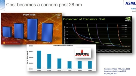
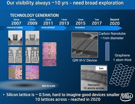
This advantage comes very natural for regular layout fabrics such as memory, but it is also available for logic circuits. The driver for this advantage is the escalating costs of lithography in state of the art IC. The following charts illustrate the impact of dimensional scaling on lithography costs.





 RSS Feed