Looking back at the past year we are thankful to see now that momentum building for monolithic 3D ICs. As stated in our company's latest blog post, in retrospective we can say thanks and looking forward to the future.
|
Happy Holidays!
Looking back at the past year we are thankful to see now that momentum building for monolithic 3D ICs. As stated in our company's latest blog post, in retrospective we can say thanks and looking forward to the future.
0 Comments
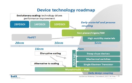
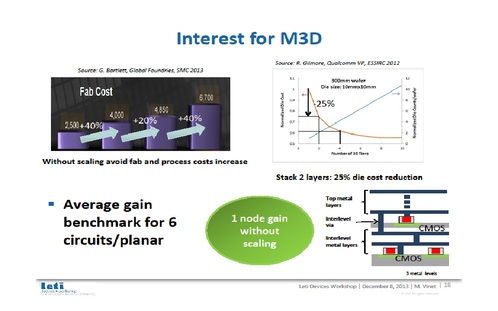
 We have a guest contribution from Zvi Or-Bach, the President and CEO of MonolithIC 3D Inc. Zvi shares latest info about the momentum that builds for monolithic 3d technology. Following last year IEDM 2012 we wrote a blog - IEDM 2012 - The Pivotal Point for Monolithic 3D IC (a good primer still well worth reading) and now, a year later, we read that Momentum Builds For Monolithic 3D ICs. Clearly dimensional scaling is not providing transistor cost reduction beyond 28 nm node, and the large fabless companies--Qualcomm, Broadcom, Nvidia, and AMD—recently reported this fact again. The industry is trying to accommodate this new reality, while still rushing to develop and adopt more advanced nodes at escalating costs and complexity. Consequently, the door has started to open for other kinds of technology that might help to maintain the industry’s overall momentum, and monolithic 3D ICs seem well positioned to do so. 3D NAND is the first segment of the industry to adopt this new path for scaling, as was reported in early August this year: Monolithic 3D is now in production: Samsung starts mass producing first 3D vertical NAND flash. A few months afterward we learned that Besang signed a license agreement with Hynix for their monolithic 3D technology, which might help Hynix to offer more competitive 3D DRAM. Then we learned that Singapore-MIT Alliance for Research Technology ordered EV Group automated production bonding system, for integrating silicon CMOS and compound semiconductor materials to enable new integrated circuits for wireless devices and power electronics. And just last week CEA Leti announced an agreement with Qualcomm to Evaluate Leti’s Non-TSV 3D Process. Thus it fitted very well for Leti to include in their presentation event done in conjunction with this year’s IEDM 2013, slides promoting monolithic 3D as an alternative to dimensional scaling as is presented in the following slide: Leti’s presentation goes even further. One can see that in the following Leti slide, monolithic 3D is positioned as a far better path to keep the industry momentum and provides the cost reduction that dimensional scaling does not provide any more. Monolithic 3D also does it with far less costly fab infrastructure and process R&D. As the slide sums it up: "1 node gain without scaling," or, as others may say, the new form of scaling is scaling up. In monolithic 3D the base stratum might be SOI or bulk, but the upper strata are naturally SOI. It is therefore fitting that the traditional IEEE conference on SOI has extended its scope and now calls itself S3S: SOI technology, 3D Integration, and Subthreshold Microelectronics. The Subthreshold section fit just as well as was presented in this year's plenary talk by Prof. Bob Brodersen - "The most important technology requirement - Continue the increase in the number of transistors (feature scaling, 3D integration,...)". The 2014 S3S conference is scheduled for October 6-9, 2014 at the Westin San Francisco Airport. This new unified conference will help us to improve efficiency and establish this conference as a world class international venue to present and learn about the most up-to-date trends in CMOS and post-CMOS Scaling. The conference will provide both educational and cutting edge research in the monolithic 3D and other supporting domains. Please mark your calendar for this opportunity to contribute and learn about the new and exciting monolithic 3D technology, a technology that is well positioned to keep the semiconductor industry's momentum now that dimensional scaling has reached its diminishing return phase.
|
Search Blog
Meet the BloggersFollow usRecommended LinksRecommended Blogs
Archives
July 2024
Categories
All
|


 RSS Feed