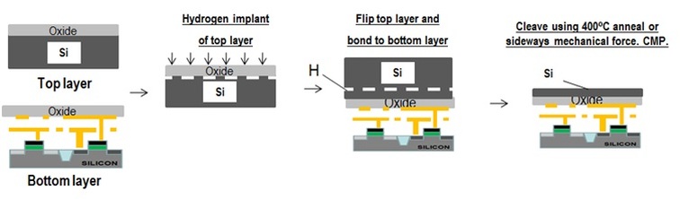
Ion-Cut: The Building Block of our Monolithic 3D Technologies
Ion-cut, also known as layer transfer, has been the dominant method to produce SOI wafers for the past two decades. Multiple thin (10s – 100s nanometer scale) layers of virtually defect free Silicon can be created by utilizing low temperature (<400C) bond and cleave techniques, and placed on top of active transistor circuitry. All our monolithic 3D approaches leverage this well-understood, manufacturing-friendly process.
For more details, please see
[1] Our blog-post on cost of ion-cut, July 2011.