Monolithic 3D Inc., the Next Generation 3D-IC Company
  • Home
  • Technology
    • Technology
    • Papers, Presentations and Patents
    • Overview >
      • Background
      • Why Monolithic 3D?
      • Paths to Monolithic 3D
      • Applications
    • Ion-Cut: The Building Block
    • Monolithic 3D Logic >
      • RCAT
      • HKMG
      • Laser Annealing
      • RCJLT
      • 3D Embedded RAM
      • 3D Gate Array
      • FPGA
      • Ultra Large Integration - Redundancy and Repair
    • Monolithic 3D Memory >
      • 3D DRAM
      • 3D Resistive Memories
      • 3D Flash
    • Monolithic 3D Electro-Optics >
      • 3D Image Sensors
      • 3D Micro-Displays
  • 3D-IC Edge
    • 3D-IC Edge
  • News & Events
    • News & Events
    • S3S15 Game Change 2.0 Video/P
    • Webcast
    • Webinar
    • Press Releases
    • In the News
    • Upcoming Events
  • About Us
    • About Us
    • History
    • Team
    • Careers
    • Contact Us
  • Blog
  • Simulators

Three-Dimensional Gate Array

Follow link for presentation on: Derivatives Gate Array.
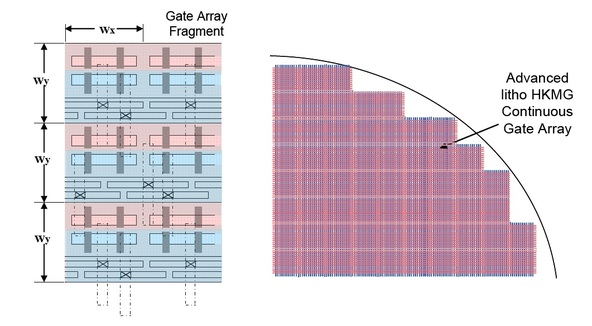
Picture

Technology

  • Dense High Performance HKMG Gate Array with continuous N/P strips
  • Layer Transfer with Ion Cut for 3D stacking
  • Gate Replacement after Ion Cut
  • Alignment error guaranteed smaller than Wx and Wy independent of Layer Transfer
  • Multiple stacking for ultra dense arrays
  • Mix of GA and Memory wafers in stack
  • Unidirectional layout
  • Continuous Array style of wafer patterning
  • Etching scribe lines per application demand

Benefits

  • Very high density Gate Array terrain
  • Easy patterning with unidirectional layout
  • Continuous Array allows flexible dicing for variable-sized chips
  • 3D stacking allows flexible ratio between memory and logic
  • 3D stacking allows ultra-high device density
  • Single mask set for a complete range of Gate Arrays
Picture
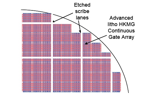
Inexpensive Arbitrary‐sized Gate Array Manufacturing
Picture
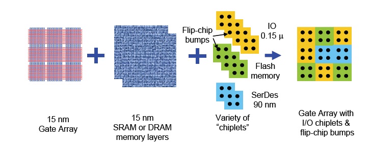
Chip‐on‐Wafer I/O Chiplet Assembly

Technology

  • Wafer-scale Continuous Array with custom-etched scribe lines
  • Chiplets with I/O, analog functions, etc.
  • Chiplets contain flip-chip bumping
  • TSV or microbump-based Wafer-on-Wafer and Chip-on-Wafer 3D stacking

Benefits

  • Arbitrary-sized Gate Array
  • Flexible I/O and analog function configuration
  • Possible re-use of older prequalified silicon I/O together with most advanced logic technology
  • Gate Array family no longer needs costly multiple mask sets
© Copyright MonolithIC 3D Inc. , the Next-Generation 3D-IC Company, 2012 - All Rights Reserved, Patents Pending