Monolithic 3D Inc., the Next Generation 3D-IC Company
  • Home
  • Technology
    • Technology
    • Papers, Presentations and Patents
    • Overview >
      • Background
      • Why Monolithic 3D?
      • Paths to Monolithic 3D
      • Applications
    • Ion-Cut: The Building Block
    • Monolithic 3D Logic >
      • RCAT
      • HKMG
      • Laser Annealing
      • RCJLT
      • 3D Embedded RAM
      • 3D Gate Array
      • FPGA
      • Ultra Large Integration - Redundancy and Repair
    • Monolithic 3D Memory >
      • 3D DRAM
      • 3D Resistive Memories
      • 3D Flash
    • Monolithic 3D Electro-Optics >
      • 3D Image Sensors
      • 3D Micro-Displays
  • 3D-IC Edge
    • 3D-IC Edge
  • News & Events
    • News & Events
    • S3S15 Game Change 2.0 Video/P
    • Webcast
    • Webinar
    • Press Releases
    • In the News
    • Upcoming Events
  • About Us
    • About Us
    • History
    • Team
    • Careers
    • Contact Us
  • Blog
  • Simulators

Game Changing Breakthrough - IEEE S3S 2014

9/10/2014

0 Comments

 
Picture
We have a guest contribution from Zvi Or-Bach, the President and CEO of MonolithIC 3D Inc. Mr. Or-Bach discusses about the emergence of monolithic 3D technology in the near future.

The coming 2014 IEEE S3S conference (October 6-9) is first one to focus on the emergence of monolithic 3D technology. It is fitting that it would be the forum at which a key decisive breakthrough for monolithic 3D IC ("M3DI") technology will be presented. This game changing breakthrough is the first ever monolithic 3D flow that allows a fab to build a monolithic 3D integrated device while using the fab’s existing transistor process flow, without the need to develop and qualify new transistors and a new transistor formation flow.

Recent blogs such as Established Nodes Getting New Attention and Moore's Lag Shifts Paradigm of Semi Industry have articulated the building up of interest in SOI, Sub-threshold and 3D IC technologies. The IEEE S3S is the conference to learn and get updated on these technologies and M3DI is that newest part integrated into the conference. The 3D part of S3S 2014 will have a full day of tutorial presentations by leading researchers in the space, a full session of invited papers, and will conclude with a session dedicated to discussing the most recent breakthroughs in the field.

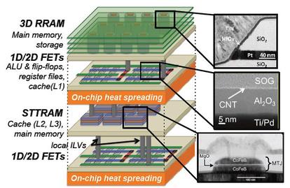
The M3DI short course will cover alternative process flows that enable M3DI, discuss the challenges and solutions to removal of the operating heat of monolithic 3D stacks, and describe the range of powerful advantages provided by M3DI. Subsequently, Prof. Sung Kyu Lim of Georgia Tech will cover EDA for M3DI. This will be followed by broad coverage of M3DI for memory applications by two leading experts in the field, Akihiro Nitayama of Toshiba/Tokohu University and Deepak Sekar of Rambus. M3DI provides unparalleled heterogeneous integration options which will be covered by Prof. Eugene Fitzgerald of MIT and SMART Lee Institute of Singapore describing the integration of silicon with other crystals for electro-optic device integration. The short course will conclude with Prof. Philip Wong of Stanford, who leads research efforts to integrate silicon with carbon nanotube and advanced 2D transistors layered with memory such as STT-MRAM and RRAM.
Picture
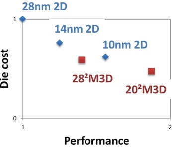
In the special invited 3D Hot Topics session we expect to get a full spectrum of the latest progress in the field. Particularly worth noting is the recent progress on the work done by CEA Leti with involvement of ST Micro, IBM and supported by Qualcomm. This work shows both a practical path to monolithic 3D IC and cost analysis of the monolithic 3D advantages. The following chart illustrates the reasons for the high interest in the technology.
Picture
And then there is a great dessert to this 3D feast. On Thursday afternoon, in the 3D New Developments session, a game changing breakthrough technology will be presented. Leveraging the breakthrough progress in wafer bonding technology, presenting for the first time ever a monolithic 3D flow using existing fab transistor process. Any fab could utilize this breakthrough to provide far better products at minimum capital and R&D investment. This game changing flow removes the historical differentiation between sequential and parallel 3D, and should significantly reduce the time for monolithic 3D adoption throughout the semiconductor industry.

For a postprandial enjoyment, CEA Leti will present in the Late News session a fully constructed M3DI SOI device, and IBM will present its Multi Stacked Memory Wafer technology.

More information is available on the conference site: S3S Conference 2014

submit to reddit
0 Comments

Intel vs. Intel

8/13/2014

1 Comment


Will Intel 14 nm Continue the Historical Cost Reduction Curve

Picture
We have a guest contribution from Zvi Or-Bach, the President and CEO of MonolithIC 3D Inc. Mr. Or-Bach discusses about Intel's decision to continue with its historical cost reduction curve.
Along with many in the industry, we were pleased to see the release of Intel's 14 nm technical information on Aug. 11 - Intel Outlines 14nm, Broadwell. It does look like after an extended delay the 14 nm is coming and with it some clarity about the Intel 14 nm technology. Clearly this recent 14 nm information release is being presented by Intel to continue the historical trend of cost reduction and dimensional scaling. Undoubtedly, Intel’s 14 nm technology is a significant technological achievement and deserves full respect and appreciation. Yet, if one takes a closer look at this information, and especially with respect to prior information provided by Intel, there is room for some clarification.  

The above EE Times article provides the following numbers released by Intel on August 11:
"Compared to Intel's 22nm process, it will have:

  • 42nm fin pitch, down .70x
  • 70nm gate pitch, down .78x
  • 52nm interconnect pitch down .65x
  • 42nm high fins, up from 34nm
  • a 0.0588 micron2 SRAM cell, down .54x
~0.53 area scaling compared to 22nm"
Let’s review the SRAM cell size of 0.0588µm². Yes, it is the smallest published size for a SRAM bitcell we have seen so far. Yet in our blog Intel vs. TSMC: An Update we wrote:  "Accordingly, the 14nm node 6T SRAM size for conventional dimensional scaling should be 0.092 * (14/22)² =0.037 sq. micron. And if Intel can really scale more aggressively to compensate for the extra capital costs then their 6T SRAM at 14nm, it should be about 0.03 sq. micron or even smaller."

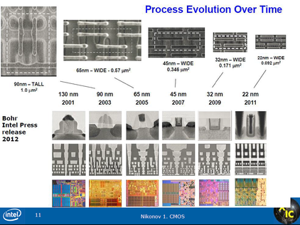
From Intel’s 2012 information release:
Picture
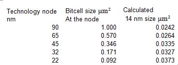
In the following table we calculated the expected bitcell size for 14nm according to simple dimensional scaling rules based on each of the bitcell sizes for each of the technology nodes in the above 2012 chart:
Picture
The above table indicates that SRAM bitcell scaling has been a challenge for some time but at 14 nm it broke totally away!

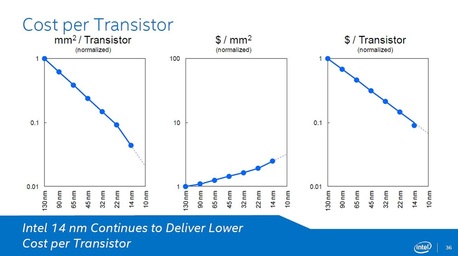
The recent Intel presentation argues for the continuation of historical scaling cost reduction to the 14 nm node as illustrated in the following Intel slide:

Picture
The graph in the middle shows the exponential increase in wafer cost with scaling; however, the argument made is that the more than 2X increase in transistor density compensates for the increase in wafer cost, resulting with the rightmost chart showing a consistent reduction in cost per transistor.

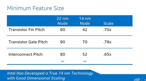
But the following Intel chart does not show a better than 2X density increase from 22nm to 14nm:

Picture
Actually the basic transistor gate pitch indicates only a x1.64 increase in transistor density.

As well, this is before accounting for the increase in RC associated with the narrower metal lines. This would require insertion of many more buffers and repeaters, further reducing the effective density increase.

Furthermore, back to the SRAM bitcell. The announced size for the Intel 14nm bitcell as presented above is not going to help offset the increase in wafer cost.

So it seems this would be a subject matter for more comments and blogs. However, I see no reasons to change my prior statements published in the EE Time blog titled: 28nm – The Last Node of Moore's Law.

1 Comment

CEA-Leti: Monolithic 3D is the solution for further scaling

7/22/2014

0 Comments

 
Picture
We have a guest contribution today from Brian Cronquist, MonolithIC 3D Inc.'s VP of Technology & IP. Brian discusses about monolithic 3d technology as the solution for future scaling as proposed by CEA-Leti.
Hughes Metras, Leti’s VP of Strategic Partnerships North America, introduced the lead talk at their SemiconWest 2014 Leti Day about monolithic 3D technology as the “solution for scaling.” Hughes presented the Leti device technology roadmap which showed monolithic 3D (M3D) as an alternative to scaling from the 2Xnm nodes to well past 5nm. Here’s the important piece of that roadmap, which highlights the partnership with Qualcomm (ST and IBM helped with some of the work as well):
Picture
The lead talk was given by device scientist Olivier Faynot, Leti’s Device Department Director.  He titled his talk “M3D, a disruptive approach for further scaling,” and began with why the industry needs a solution for scaling.

Most in the industry are in agreement that scaling past the 22nm node, while still quite technically feasible, has priced itself out of most markets. Olivier discussed the what (transistor costs are no longer decreasing) and the why (litho cost escalation and connectivity inefficiencies of energy and delay). And then he made the statement: “if we just keep the current (2Xnm) technology, we can go farther in cost scaling.” [note: see the following blogs and comments for more info on this crucial topic:  Tech Design Forums summary "3D and EDA need to make up for Moore’s Law, says Qualcomm" and Zvi-Or-Bach’s EETimes blogs Qualcomm Calls for Monolithic 3D IC and  28nm - The Last Node of Moore's Law.]

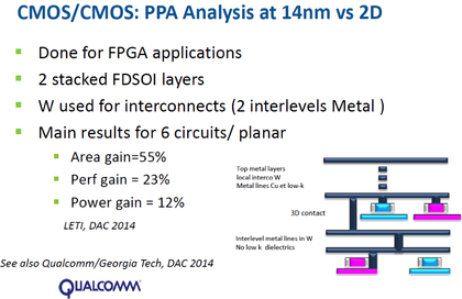
Oliver showed a summary of a DAC2014 paper and a Qualcomm/GeorgiaTech DAC2014 paper Power/Performance/Area analysis of M3D for an FPGA:

Picture
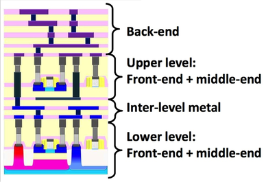
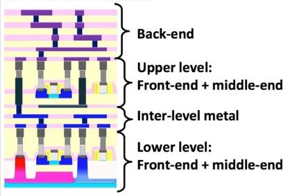
The solution is to build the stack sequentially, in a monolithic fashion. Olivier described their monolithic 3D, or sequential 3D, process flow where the lower-level (first layer) of transistors and its interconnect are conventionally made, then inter-level metal is crafted to help the vertical interconnection, and then a second layer of monocrystalline silicon is layer transferred and oxide-oxide low temperature bonded to the top of the inter-level metal dielectric. This is a blanket layer so there are no alignment issues such as those suffered by the thick layer and pre-made (TSV) parallel processing flows. The layer that is transferred in M3D is very thin (10-200nm final), so that direct alignment thru that thin layer to the lower level alignment marks can be made with conventional equipment and achieve conventional alignment tolerances (single digit nanometers).

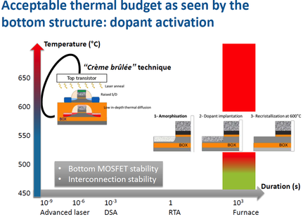
Now upper-level transistors are formed utilizing SPER (Solid Phase Epitaxial Regrow) for junction doping at 475-600°C and other lower (<400°C) temperature processing for gate stacks, etc. The upper-level and inter-level vertical interconnect is then processed, again with full alignment capability to the lower layer. Note that the lower level transistor Ni salicides are stabilized with platinum co-deposition and fluorine/tungsten implantation to enable their survival at the 475-600°C SPER thermal exposure.
Picture
Oliver also talked about using laser annealing to activate implanted dopants and repair damages during upper-level transistor processing. He called the laser (pulsed and short wavelength) option of solving the thermal challenge of monolithic 3D as the “crème brûlée” of methods and they were ‘seeing good results.’ Hopefully we will see published data soon. For more information on SPER and laser processing please see my recent blog Monolithic 3DIC: Overcoming silicon defects.
Picture
Oliver was also asked in the Q&A if stress was a big issue. He replied that stress was not an issue, rather, the biggest challenges were integration ones (how to form a low temp top transistor, stability of the local interconnect level, and the bottom transistor salicide stability). Olivier was asked in the Q&A what the observed performance differences were between the upper-level and lower-level transistors. He replied” Currently we are achieving 95% (of the lower for the upper). We believe we can make 100%.”

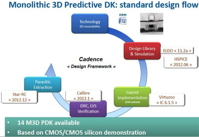
Leti has a 14nmPDK ready to go for those who want to design a test circuit in their monolithic 3D flow. They have ELDO, HSPICE, Virtusoso, Calibre, StarRC, etc. files available.
Picture
Not too surprisingly, the Qualcomm logo showed up on some of the Leti presentation slides. Back in December 2013, Leti signed an agreement to work with Qualcomm – Qualcomm to Evaluate Leti’s Non-TSV 3D Process. ST and IBM have also been working with Leti in various aspects, for example, IBM & Leti used COMPOSE3 to simulate a monolithic InGaAs nFET monolithically over a SiGe pFET on SOI.

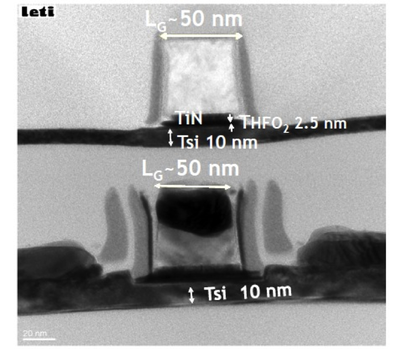
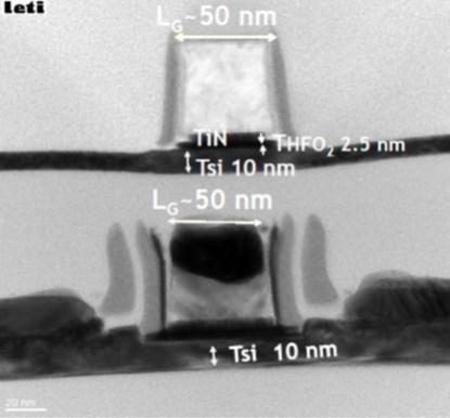
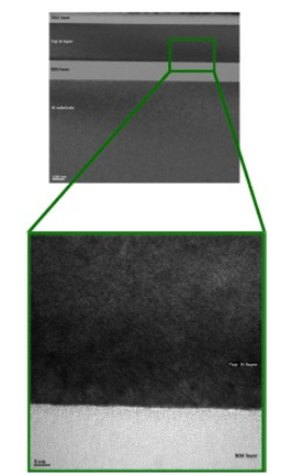
CEA-Leti has been busy working on processing flows to enable monolithic 3D devices since before 2009. Perrine Batude won the 2009 Roger A. Haken Best Student Paper Award for the IEDM 2009 paper entitled, “Advances in 3D CMOS Sequential Integration,” where she showed results for a sequentially processed P over N (no metal between transistors layers) testchip Batude’s 2011 IEDM paper showed a 50nm 3D sequential structure on 10nm channel silicon:

Picture
CEA-Leti also opened a complete 300mm fab extension dedicated to 3D-integration applications, both parallel and monolithic, with an inauguration event in January 2011. As well, back in December 2013, Soitec and CEA renewed their long-standing partnership for an additional five years.

Clearly, monolithic 3D integration has a very important role for the future of the semiconductor industry. I would like to invite you to the IEEE S3S Conference: SOI technology, 3D Integration, and Subthreshold Microelectronics. The 2014 S3S Conference will be held October 6-9, 2014 at the Westin San Francisco Airport. This would be a great opportunity to learn more about monolithic 3D technology, with five invited presentations covering topics from design tools to monolithic 3D NAND and other 3D memories. CEA Leti will present their work on CMOS monolithic 3D IC. Researchers from MIT and Stanford will present manufacturing monolithic 3D devices with materials other than silicon.
See you there!

submit to reddit
0 Comments

Paradigm shift in semi equipment – Confirmed

7/21/2014
0 Comments

 
Picture
We have a guest contribution from Zvi Or-Bach, the President and CEO of MonolithIC 3D Inc. Mr. Or-Bach discusses about the shift in semi equipment, a paradigm confirmed lately.

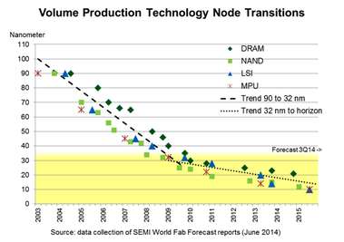
Our blog Paradigm shift: Semi equipment tells the future, was focused on the quote: “Now more money is spent on upgrading existing facilities, while new capacity additions are occurring at a lower pace.” And now, just prior to Semicon West, we have the conclusion of the recent SEMI’s World Fab Forecast — Technology Node Transitions Slowing Below 32 nm. The SEMI World Fab Forecast uses a bottom-up approach methodology, providing high-level summaries and graphs, and in-depth analyses of capital expenditures, capacities, technology and products by fab. The following chart illustrates this new paradigm:
Picture
The report states: “The cost per wafer has become an increasing concern below the 32nm node.   The expected cost reduction benefit of production at smaller nodes is diminishing and is not keeping pace with the scaling benefits in many cases.  This has widespread and fundamental implications for an industry long following the cadences of Moore’s Law… These may be contributing factors as to why some volume fabs are exhibiting a lag in beginning production of new technology node.  Now evident quantitatively for the first time, there is evidence of a clear slowdown in volume production scaling of leading technology node transitions.” (emphasis added)

It is fitting to point to the comment made to EE Times coverage on Semicon West – 13 Things I Heard at Semicon West: “No matter what Intel says, Moore’s Law is slowing down,” said Bob Johnson, a semiconductor analyst for Gartner. “Only a few high-volume, high-performance apps can justify 20 nm and beyond.” He sees problems ahead for logic chips in general,” and to follow with quotes from another EE Times article – Silicon Highway Narrows, Twists: “Most foundries have yet to start buying the capital equipment needed for the 14/16 nm node, which for many will be the first to support FinFETs, says Trafas of KLA-Tencor. Gear companies hope the orders start coming in the fall…Indeed, he says, one of the big questions many capital equipment execs will bring to this year’s Semicon West event on July 7 is, “When will the 16/14 nm investments begin?”

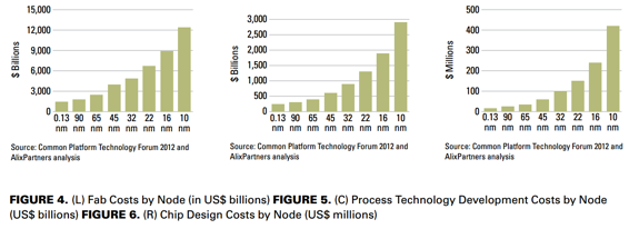
Since the 65 nm node, escalating costs of fab and process technology development and design, as illustrated in the chart below, put a huge pressure on the industry.

Picture
These escalating costs drove consolidation in the industry, cutting down to a handful the vendors who are still pursuing the leading edge.

At the recent (2014) SST ConFab in Las Vegas Bill McClean shared his annual report on Major trends shaping the future IC Industry. Bill reports: “Over the last two decades, the percentage of capex being spent by the top 5 has steadily increased to its current 70% with the big three of Samsung, Intel and TSMC being responsible for over 50%.” This is illustrated by the following chart.
Picture
Clearly the escalating costs drove out most but the largest vendor, but now we are facing the ”second punch” – the diminishing returns.

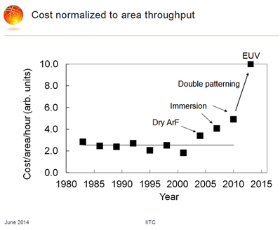
In the recent ITC conference Harry J. Levinson of GlobalFoundries in his talk: Lithography Issues for High Volume Manufacturing” presented the following chart:
Picture
The dramatic increase of lithography cost eats away the historical transistor cost reduction resulting from reduced dimensions, as we reported in our blog Qualcomm: Scaling down is not cost-economic anymore – so we are looking at true monolithic 3D. Quoting Qualcomm “One of the biggest problems is cost. We are very cost sensitive. Moore’s Law has been great. Now, although we are still scaling down it’s not cost-economic anymore. It’s creating a big problem for us.” Accordingly we detailed in our blog that Moore’s Law has stopped at 28nmand following nodes would not provide lower transistor cost, and for most application will result in higher SoC costs.

We should not be surprised that the production ramp up below 28 nm is extremely slow. There is too much money involved to put it into the wrong place.

Going back to the SEMI World Fab Forecast, the authors ask “What’s next?” and respond: “Many in our industry are grappling with what to do as they have perceived the coming slowdown in technology node transitions.  IC manufacturers are now increasingly looking outside of conventional lithography and wafer size scaling approaches to pick up the pace of cost reduction while increasing transistor density and performance. Using memory as an example, to cope with increasing challenges in continuing to scale 2D, memory companies are looking into 3D.”

So the memory vendors already started shifting their Capex budget to scaling up with 3D NAND, instead of scaling to smaller dimension. Recently Qualcomm announced their collaboration with SMIC – China’s SMIC-Qualcomm 28-nm Deal: Why Now? – indicating more capacity build-up for 28 nm with looking forward to scaling up with monolithic 3D for logic as well. Quoting: ”Going forward, SMIC will also extend its technology offerings on 3DIC and RF front-end wafer manufacturing in support of Qualcomm”.

It is clear now that we are seeing a paradigm shift in the semiconductor equipment industry. After many decades of relentless dimensional scaling every two years, there is a change coming and we see a lower rate of dimensional scaling and exploration of other paths, to keep industry’s march on. We do believe that the next few decades will be about scaling with 3D Integration and we are pleased to see many others thinking the same.

The 2014 S3S Conference is scheduled for October 6-9, 2014, at the Westin San Francisco Airport, and would be a great opportunity to learn more about monolithic 3D technology, with five invited presentations covering topics from design tools to monolithic 3D NAND and other 3D memories. CEA Leti will present their work on CMOS monolithic 3D IC. Researchers from MIT and Stanford will present manufacturing monolithic 3D devices with materials other than silicon.
submit to reddit
0 Comments

Monolithic 3D: A Disruptive Approach for Further Scaling

7/14/2014
0 Comments

 
Picture
We have a guest contribution today from Brian Cronquist, MonolithIC 3D Inc.'s VP of Technology & IP. Brian discusses about monolithic 3d technology for future scaling.

At the CEA-Leti Day July 8 during Semicon West, Hughes Metras, Leti's vice president of strategic partnerships for North America, introduced the lead talk about monolithic 3D technology as the "solution for scaling." The Leti device technology roadmap that Hughes presented showed monolithic 3D (M3D) as an alternative to scaling from the 2Xnm nodes to past 5 nm.Olivier Faynot, Leti's device department director and a well-known device scientist (with more than 170 papers/publications), entitled his talk "M3D, a disruptive approach for further scaling" and started with why the industry needs such a solution.

The majority of people in the industry agree that scaling past the 22nm node, though still quite technically feasible, has priced itself out of most markets. Faynot discussed the "what" (transistor costs are no longer decreasing) and the "why" (litho cost escalation and connectivity inefficiencies of energy and delay). Then he said, "If we just keep the current [2Xnm] technology, we can go farther in cost scaling."

Tech Design Forum's summary of a Qualcomm executive's DAC 2014 keynote offers more information on this crucial topic. So do a pair of EE Times blogs by Zvi Or-Bach.
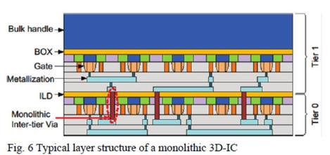
The solution is to build the stack sequentially in a monolithic fashion. (See Monolithic 3D IC Technologies.) Faynot described a process flow wherein the lower level (first layer) of transistors and its interconnect are made conventionally, some interlevel metal is crafted to help the vertical interconnection, and a second layer of monocrystalline silicon is layer transferred and oxide-oxide bonded at low temperature to the top of the interlevel metal dielectric. This is a blanket layer, so there are no alignment issues such as those suffered by the thick layer and pre-made (TSV) parallel processing flows. The layer that is transferred in M3D is very thin, so that direct alignment to the lower-level alignment marks can be made with conventional equipment, and conventional alignment tolerances (single-digit nanometers) can be achieved.

Upper-level transistors are formed utilizing solid-phase epitaxial regrow (SPER) for junction doping at 475-600°C and lower-temperature processing (less than 400°C) for things like gate stacks. The upper-level and inter-level vertical interconnect is then processed, again with full alignment capability to the lower layer. (Note that the lower-level transistor salicides are stabilized with platinum and fluorine/tungsten implantation to enable their survival at the 475-600°C SPER thermal exposure.)

In the Q&A session, Faynot was asked what the observed performance differences were between the upper-level and lower-level transistors. "Currently, we are achieving 95%" of the lower for the upper, he said. "We believe we can make 100%."
Picture
He also talked about using laser annealing to activate implanted dopants and repair damages during upper-level transistor processing. The laser option of solving the thermal challenge of monolithic 3D is the "crème brûlée" of methods, and Leti is "seeing good results." Hopefully, we will see published data soon. My recent Solid State Technology blog offers more information on SPER and laser processing.

Faynot was also asked if stress is a big issue. He replied that stress is not an issue. Rather, the biggest challenges are integration ones.

Leti has a PDK ready to go for those who want to design a test circuit in their monolithic 3D flow. The company has ELDO, HSPICE, Calibre, StarRC, and other files available, and it has said that monolithic 3D offers savings of at least 55% on area, 23% on performance, and 25% on power over 2D.

Not too surprisingly, the Qualcomm logo showed up on some of the Leti presentation slides. Back in December, Leti signed an agreement to work with Qualcomm. ST and IBM have also been working with Leti in various areas.

Since before 2009, CEA-Leti has been busy working on processing flows to enable monolithic 3D devices. Perrine Batude won the 2009 Roger A. Haken Best Student Paper Award for the IEDM 2009 paper "Advances in 3D CMOS Sequential Integration" (subscription required). In that paper, she and her co-authors showed results for a sequentially processed P over N (no metal between transistor layers) test chip. In an IEDM 2011 paper, she and her colleagues showed a 50nm 3D sequential structure on 10nm channel silicon, illustrated below.

Picture
CEA-Leti also opened a complete 300mm fab extension dedicated to 3D-integration applications -- both parallel and monolithic -- with an inauguration event in January 2011. In December 2013, Soitec and CEA renewed their longstanding partnership for an additional five years.

Clearly, monolithic 3D integration has a very important role for the future of the semiconductor industry. It is therefore fitting that the traditional IEEE conference on SOI has extended its scope and now calls itself S3S: SOI technology, 3D Integration, and Subthreshold Microelectronics. The 2014 S3S Conference is scheduled for Oct. 6-9 at the Westin San Francisco Airport. CEA-Leti will present its work on CMOS monolithic 3D IC. Researchers from MIT and Stanford will present manufacturing monolithic 3D devices with materials other than silicon. With five invited presentations covering topics from design tools to monolithic 3D NAND and other 3D memories, this would be a great opportunity to learn more about monolithic 3D technology.

-- Brian Cronquist is vice president of technology and IP at MonolithIC 3D Inc. He has 35 years of semiconductor industry experience as senior director of technology development and foundry at the nonvolatile FPGA provider Actel (now Microsemi), starting and building Chartered Semiconductor-Singapore (now GlobalFoundries), running startup wafer fab engineering teams at Sierra Semiconductor (now PMC-Sierra), and developing process technology at AMI and Synertek/Honeywell. He has published more than 100 technical papers in the fields of semiconductor microelectronic radiation effects and hardening, as well as new 3D-IC, logic, antifuse, and flash processes, devices, and reliability. He holds more than 60 issued/pending patents.
submit to reddit
0 Comments

Monolithic 3DIC: Overcoming silicon defects

7/8/2014

0 Comments

 
Picture
We have a guest contribution today from Brian Cronquist, MonolithIC 3D Inc.'s VP of Technology & IP. Brian discusses about overcoming silicon defects in monolithic 3d.

As dimensional scaling has reached the diminishing return era there is a buildup of interest in monolithic 3D as an alternative path forward. Both memory and logic vendors are moving to monolithic 3D. The memory vendors are in transition to 3D NAND and Samsung has already announced mass production of their V-NAND. BeSang has been working in monolithic 3D memory for many years and has recently signed a license agreement with SK Hynix. And now, in the logic arena, Qualcomm has voiced a call for monolithic 3D “to extend the semiconductor roadmap way beyond the 2D scaling.” The reason is economic: … “although we are still scaling down, it’s not cost-economic anymore” (Karim Arabi, DAC 2014).

A key aspect of monolithic 3D is engineering the second layer to be especially thin, on the order of 100nm or less. This provides for tiny (10s of nm diameter) vertical connections which are dense, manufacturable, and stress-free.  They can be manufactured with well understood processing as these vertical connections would look very much like the metal to metal vias that the industry has been making for decades. This avoids the 10+ micron sized TSVs of parallel 3D and their associated reliability hazards, process cost, Keep Out Zones, and ‘newness risk’.

When performance is important, single crystal silicon based transistors are the way to go for stacked layers. So far, it seems that the best technique to form such thin mono-crystal layers with the required thickness control is to use the volume production and well proven ion-cut process. Many of the high performance monolithic 3D process flows utilize ion-cut techniques, sometimes called ‘Smart-Cut’.

However, use of ion-cut creates a small number of crystal defects in the very thin single crystal layer-transferred film. I’ll talk about some techniques that may be employed to solve this but, first, let’s explore why defects are created in the ion-cut process.

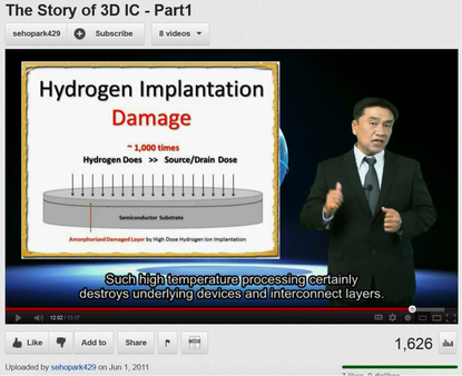
The high dosage of ions used in the process creates damage to the silicon lattice at, and near, the ion-stopping depth, such that the lattice becomes brittle there; hence, can be ‘cut’ or ‘exfoliated’ with a force (e.g., knife, water jet) or thermal anneal. After separation of the layer to be transferred from the donor substrate, this ‘donor layer’ will still have some of the silicon lattice damage from the embrittlement on one surface, and may also have some damage from the splitting process itself. Soitec, in the manufacture of SOI wafers, utilizes 1100-1200°C thermal anneals (both oxidizing and non-oxidizing) in combination with chemical-mechanical polishing (CMP) to repair the crystalline damage, as part of its SmartCut (ion-cut) process. However, these damage repair anneals are not compatible with the commonly used low melting point/hi-diffusivity interconnect metals like copper or aluminum of the lower device layer in a 3D stack. BeSang has a nice tutorial video explaining this on their website. Here’s a snapshot:

Picture
Figure 1
Further, the passage of the ions used in the ion-cut process creates a lower level of damage to the silicon lattice of the bulk of the to-be-transferred donor layer as the ions pass thru the lattice. This bulk lattice damage can cause junction leakage, and lower the performance of devices. Annealing this type of lattice damage requires temperatures of about 600°C or greater, which – again – is incompatible with the commonly used interconnect metals of the lower device layers in a 3D stack.

Now let’s look at two silicon device proven methods that are available to overcome the ion-cut induced defects and can be applied to the ion-cut layer transfer for monolithic 3D devices and  structures.

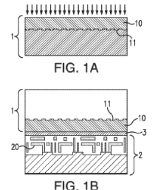
Radu et al. of Soitec, in U.S. Patent Application Publication 2013/0026663, describe a method for curing defects associated with ion-cut implantation by a CMP and then a laser anneal of the transferred singe crystal silicon layer.

Singe crystal silicon donor wafer 1 is ion-implanted with a heavy dose of hydrogen or helium ions to create a brittle region 11 as shown in Fig. 1A. Then the donor wafer is flipped over and bonded to the top of a receiver substrate 2 that may have transistors and interconnect metallization 20, shown in Fig. 1B. Layer 3 is a low thermal conductivity or thermal insulating layer that will help thermally protect the transistors and interconnect metallization 20 of substrate 2.
Picture
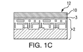
Fracturing along the brittle region 11 may be done with any number of techniques, such as mechanical knife, water or gas jet, etc., leaving behind transferred silicon layer 10. The transferred layer surface 12 may be CMP’d to remove the majority of the roughness and surface defects, resulting in Fig. 1C.
Picture
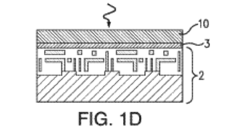
However, there are still bulk lattice damage centers in transferred silicon layer 10. Radu et al. takes care of them thermally by applying pulses of electromagnetic energy. Specifically mentioned are the pulsed lasers of Excico and JPSA.
Picture
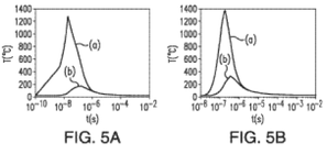
The wavelength of the irradiation is chosen such that the majority of the pulsed energy is absorbed in transferred layer 10. The low thermal conductivity or thermal insulating layer 3 minimizes the thermal diffusion from the heated transferred layer 10 to the interconnect metallization and must be designed properly to handle the thermal pulse of the layer above. Temperatures high enough to cure the ion-cut induced defects and reactivate any ion-cut deactivated dopants in transferred layer 10 can be achieved. For example, as Figs. 5A and B show, the transferred thin (0.8um in this case) silicon layer (a) may achieve a temperature well above 1000°C from the laser pulse, and the interface (b) between substrate 2 and thermal insulating layer 3 will stay well below 400°C.
Picture
Fig. 5A shows the JPSA laser at 193nm and 20ns pulse FWHM (Full-Width Half-Max) and Fig. 5B shows the Excico laser at 308nm and 160ns pulse FWHM.

We have also published work on laser annealing at 2013 IEEE 3DIC and 2013 IEEE S3S Conferences showing how scaling trends can make monolithic 3D practical and the substantial design space of the laser wavelength/energy/pulse width, top layer thickness, and shielding/thermal protection layers which can make single crystal monolithic 3D possible.

Clearly, stacking of ultra-thin layers of defect free single crystal silicon can be readily accomplished and the tools to realize this are available from at least two vendors.

At ESSDERC (43rd Solid State Device Research Conference) in September of 2013, Radu et al. in collaboration with CEA-Leti, presented a different way of obtaining low defect single crystal silicon stacks. Low temperature Solid Phase Epitaxial Re-grow (SPER) is combined with ion-cut to demonstrate defect free diodes with processing temperatures less than 500°C.

SPER utilizes a small amount of crystalline silicon as a template to re-crystallize an amorphous silicon layer at temperatures just above 475°C and can be used to activate dopants above the solubility limit.
Picture
SPER can be combined with low temperature ion-cut (SmartCut) and bonding techniques to obtain defect free single crystal devices. Donor wafer doped silicon is amorphized before bonding and ion-cut implanted to create the brittle zone, flipped and bonded to the handle, SPER processed, and then thinned to remove the End Of Range defects.
Picture
No crystalline defects were seen utilizing the usual physical means:
Picture
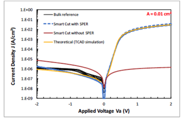
However, the tougher test to satisfy is always the electrical one. Radu showed excellent diode characteristics, resistivity, concentration and mobility recovery. Here are some of their diode I(V) curves:
Picture
I would not be surprised if demonstration of transistors is published in the near future.

So, hopefully I have given you at taste of how ready an important piece of the monolithic 3D puzzle is to delivering on its promises. Back in December 2013, Soitec and CEA-Leti renewed their long-standing partnership for five additional years. I think it is safe to say that more will be coming soon.

Give me a call or email if you want to talk more…

submit to reddit
0 Comments

The next generation technology driver - monolithic 3D

7/5/2014

0 Comments

 
Monolithic 3D moving forward for SoC and logic devices. The latest news in the semiconductor industry reveals an important strategic relationship between Qualcomm Technologies and Semiconductor Manufacturing International Corporation SMIC. The latest is one of the leading semiconductor foundries in the world and the largest and most advanced foundry in mainland China. "SMIC is further strengthening its strategic relationship with Qualcomm Technologies. SMIC will work with Qualcomm Technologies in bringing new 28nm design-ins and products for the growing mobile communication industry. Going forward, SMIC will also extend its technology offerings on 3D IC and RF front-end wafer manufacturing in support of Qualcomm Technologies". As Zvi Or-Bach, Presindet and CEO of MonolithIC 3D Inc. recently reported in our blog: "Qualcomm Calls for Monolithic 3D IC", first developing EDA with help of Georgia Tech., than support the process development at CEA Leti, and now setting up volume production with SMIC. This is the first announcement of moving to monolithic 3D for SoC and logic devices after Samsung already reported mass production of for monolithic 3D in first 3D vertical NAND flash.

Source:

- SMIC and Qualcomm Collaborate on 28nm Wafer Production in China – Solid State Magazine [http://electroiq.com/blog/2014/07/smic-and-qualcomm-collaborate-on-28nm-wafer-production-in-china/];

- China's SMIC-Qualcomm 28-nm Deal: Why Now? - EE Times [http://www.eetimes.com/document.asp?doc_id=1322988&piddl_msgid=306046#msg_306046];

submit to reddit
0 Comments

Qualcomm calls for monolithic 3D IC

6/21/2014

0 Comments

 
Picture
We have a guest contribution from Zvi Or-Bach, the President and CEO of MonolithIC 3D Inc. Mr. Or-Bach discusses about the latest news shared by Qualcomm.

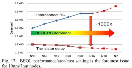
"Qualcomm is looking to monolithic 3D and smart circuit architectures to make up for the loss of traditional 2D process scaling as wafer costs for advanced nodes continue to increase." Speaking in a keynote at DAC 2014 in San Francisco, vice president of engineering Karim Arabi, is reported to argue that 3D and EDA need to make up for Moore’s Law.This was the third time in the past year that Qualcomm executives have made such a call at major industry conferences. At IEDM 2013 Geoffrey Yeap, Qualcomm VP of Technology, stated in his invited talk: "As performance mismatch between transistors and interconnects continue to increase, designs have become interconnect-limited. Monolithic 3D (M3D) is an emerging integration technology poised to reduce the gap significantly between transistors and interconnect delays to extend the semiconductor roadmap way beyond the 2D scaling trajectory predicted by Moore’s Law." Yeap provided the following chart for the growing gap between transistor delay and interconnect delay

Picture
Figure 1
Earlier that year, Robert Gilmore, Qualcomm VP Engineering, in his invited talk at VLSI 2013 (Kyoto, Japan), used almost the same words and provided the following illustration (note the wafer is face-down):
Picture
Figure 2
Clearly there seems to be a concentrated effort by Qualcomm to promote the development and adoption of monolithic 3D.

Qualcomm has done more than just talking. It has been investing in monolithic 3D development tools with institutions such as Georgia Tech (see their GTCAD LAB website reporting technology transfer in 2012 and 2014). Qualcomm has been filing patents in this area and recently announced an agreement to work with CEA-Leti - Qualcomm to Evaluate Leti’s Non-TSV 3D Process

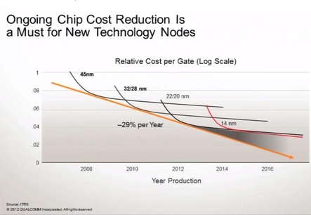
It would seem that the number one motivation behind these efforts is Qualcomm’s concern about future cost reductions. Early in 2012 Jim Clifford, Qualcomm's VP and GM (at that time), in his plenary talk at the SPIE conference titled - A Mobile Wireless Phenomenon: A Continued Need for Advanced Lithography, made it very clear with his second slide. At that time there were already some concerns with EUV’s rollout schedule. Jim called on the conference attendees to make sure to solve the escalation of advanced lithography cost, which was already dominating more than 50 % of the overall advanced device cost. Jim presented the following curve, showing the historical 29% cost reduction per year, and the looming problem with the production cost beyond 28 nm.
Picture
Figure 3
 Jim than said: "If the next node doesn't cost less than the last node we got a problem because I don't think the demand will be there." Well it is now clear that EUV is not ready and that dimensional scaling below 28nm will require double and triple lithography with its associated extra costs.

Back to the DAC 2014 keynote: Arabi explained: “Mobile is becoming a centre of gravity for the user. It is providing a unique opportunity ... but it becomes a challenge to develop because you have to integrate them at lower power and low cost as well ... One of the biggest problems is cost. We are very cost sensitive. Moore’s Law has been great. Now, although we are still scaling down, it’s not cost-economic anymore. It’s creating a big problem for us.” As we reported in our recent blog, 28nm – The Last Node of Moore's Law, dimensional scaling below 28 nm will result in increasing device cost. This was echoed multiple times at this DAC by other keynote speakers such as Hossein Yassaie, CEO of Imagination Technologies, who said: “Moore’s Law is really over from my point of view. It’s not that it can’t scale, it’s that the cost is not going down anymore".
Picture
Figure 4
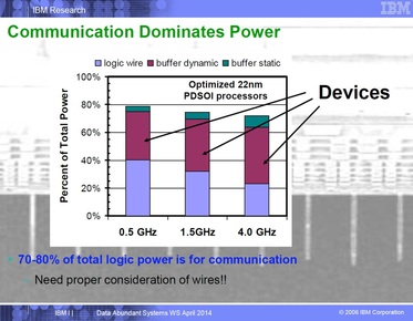
 And cost is not the only problem with dimensional scaling. The following IBM slide illustrates that interconnect now dominates device power.   
Picture
Figure 5
Interconnect’s effect on power is just getting worse with dimensional scaling. Arabi also stated in his DAC keynote: “Interconnect RC is inching up as we go to deeper technology. That is a major problem because designs are becoming interconnect-dominated. Something has to be done about interconnect. What needs to be done is monolithic three-dimensional ICs ... So we are looking at true monolithic 3D. You have normal vias between different stacks. Then interconnect lengths will be smaller than with 2D. If we can connect between layers the delay becomes smaller. This is a technology for the end of the decade, but it can give us an advantage of one process node, with a 30 per cent power saving and a 40 per cent gain in performance.”

Clearly, monolithic 3D integration has a very important role for the future of the semiconductor industry. It is therefore fitting that the traditional IEEE conference on SOI has extended its scope and now calls itself S3S: SOI technology, 3D Integration, and Subthreshold Microelectronics. The 2014 S3S conference is scheduled for October 6-9, 2014 at the Westin San Francisco Airport. This would be a great opportunity to learn more about monolithic 3D technology with 5 invited presentations covering topics from design tools to monolithic 3D NAND and other 3D memories, CEA Leti will present their work on CMOS monolithic 3D IC, and researchers from MIT and Stanford will present manufacturing monolithic 3D devices with materials other than silicon.
submit to reddit
0 Comments

FPGA as ASIC Alternative: Past and Future

4/28/2014

1 Comment

 
Picture
We have a guest contribution from Zvi Or-Bach, the President and CEO of MonolithIC 3D Inc. Mr. Or-Bach discusses about the FPGA as ASIC Alternative. 

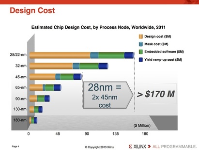
In our recent blog 28nm – The Last Node of Moore's Law we outlined the recent dramatic change that has happened after many years of cost reduction associated with dimensional scaling. It is clear now that 28 nm will provide the lowest cost per gate for years to come. In this blog we will assess the potential implications for the ASIC and the FPGA markets. Over the last two decades we have seen escalating mask set costs associated with dimensional scaling and accordingly escalating NRE costs. At the recent 2014 SEMI Industry Strategy Symposium (ISS) Ivo Bolsens, Xilinx CTO, presented the following chart of ASIC design cost escalation: 
Picture
Figure 1
The dramatic increases of ASIC design cost have had a real effect on the ASIC market, reducing the number of new designs and dramatically reducing the number of vendors serving the ASIC market.

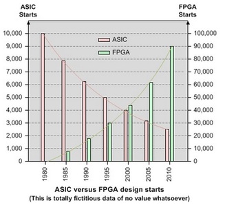
One would expect that such a trend would have a very positive effect on the FPGA market, as there is no mask-set cost associated with an FPGA design and, accordingly, far lower NRE costs per design. The following fictitious chart presented in the EE Times article: What’s the number of ASIC versus FPGA design starts?, illustrates these expectations.

Picture
Figure 2
Surprisingly, this did not really happen. The following chart presents the overall FPGA market during the last decade according to the financial results of Xilinx, Altera and Actel.
Picture
Figure 3
The FPGA market growth could be compared to the overall semiconductor market growth as presented in the chart below (the market in 2013 was $305B). Clearly the FPGA market growth during the last decade is similar to the overall semiconductor market growth, and there is no indication of any benefits from the escalating ASIC mask-set cost and its associated NRE.
Picture
Figure 4
The FPGA technology started in the mid-1980s as an alternative to the popular ASIC technology then – the Gate Array. The acronym FPGA stands for Field Programmable Gate Array. During the 1990s the Gate Array technology lost its appeal and the ~$20B Gate Array market shrunk dramatically and effectively ceased to exist. Analyst expected that this will have a dramatic positive impact on the FPGA market, which did grow some but far from the expectations. The trend of escalating NRE driven by dimensional scaling and escalating lithography costs kept on going in the 2000s and drove down the number of ASIC designs. And, again, analysts expected a huge surge in the FPGA market. Clearly, this did not happen. 

In the following we will present our theory why it did not happen and some potential implications for the future.

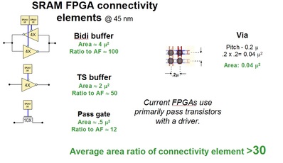
We believe that the stagnation of FPGA growth is mostly due to the inefficiency of the FPGA technology. Most FPGAs use SRAM as the programming or ‘switch’ technology. Interconnects are the dominating resource in modern designs. Within an SRAM based FPGA the programming of interconnects is implemented by an SRAM cell control of a pass transistor, driver, or bidirectional driver. The following chart illustrates the diffusion area associated for such Programmable Interconnect Cell (PIC) assessed in 45nm technology and compared to the size of mask-defined equivalent – the via. The results indicate that the cell area overhead for the SRAM PIC is over 30X when compared to a via, which does not include the additional circuit overhead area needed to program and control the SRAM PIC.
Picture
Figure 5
This number had been reported in the industry for many years. A 2007 research paper by Ian Kuon and Prof Jonathan Rose (IEEE Transaction on Computer-Aided Design of IC and System) says this clearly: “In this paper, we have presented empirical measurements quantifying the gap between FPGAs and ASICs for core logic. We found that for circuits implemented purely using the LUT based logic elements, an FPGA is approximately 35 times larger and between 3.4 to 4.6 times slower on average than a standard-cell implementation.”

This high programmability overhead suggests that many of the current ASIC designs cannot be replaced by an FPGA design. Consequently, when advanced technology NRE is too high, the alternative is to use older node ASIC technologies. Since the number one driver for cost of mask-sets and NRE is the associated capital, the cost of older technologies goes down dramatically over time. The 30X area penalty means that one could use a node that is five generations older and have a competitive solution when compared to current node FPGA. Taking into account the 60% gross margin of the FPGA companies and the overhead of using a fixed-sized device of an FPGA family rather than a custom tailored Standard Cell device, these could compensate for an additional two nodes. Looking again at the design costs as illustrated in the Xilinx chart above, we can see that at 180 nm the design costs are pretty low and the mask set costs are too small even to register on the chart.
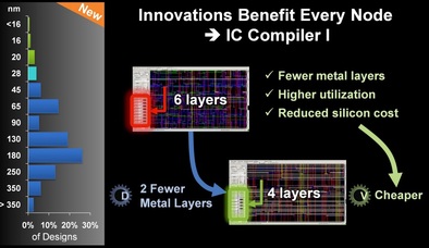
What has really happened is that many designs chose to use older node standard cells instead of an FPGA. In his last keynote presentation at the Synopsys user group (SNUG 2014) Art De Geus, Synopsys CEO, presented multiple slides to illustrate the value of Synopsys newer tools to improve older node design effectiveness. The following chart is one of them and it also includes in its left side the current distribution of design starts. One can easily see that the most popular current design node is at 180nm. Clearly even such old node provides a better product than the state of the art FPGA.  
Picture
Figure 6
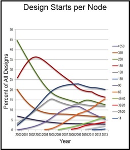
Now we understand why the escalating mask set and NRE costs have not resulted in a surge of FPGA designs but rather pushed designers to user older technology nodes that had depreciated enough to make their NRE cost less of an issue. The following chart of Design Starts per Node by IBS was recently presented in a Synopsys article "The new landscape of advanced design". It shows the design starts trend over time and, not surprisingly, indicates that designers migrate to more advanced nodes over a longer time and that the up and coming node these days is just 65 nm.
Picture
Figure 7 - Design Starts per Year (Source: IBS Dec 2012)
Recently EE Times published our blog, 28nm – The Last Node of Moore's Law. In it we presented that the 28nm node will be the end of cost reduction for dimensional scaling. Most analysts accept by now that 28 nm is going to be the lowest cost per gate for many years to come. 

There are potentially many implications of this change in Moore’s Law. One of those implications could affect the future of FPGAs.
Traditionally FPGAs have been, and still are, a technology driver of new logic technology nodes. This early adoption gave the FPGA customer a constantly better programmable platform for their designs. Now that dimensional scaling does not provide better cost, it will result in a build-up of pressure for FPGA customers to use a depreciated technology node as an alternative. Over time designers would see the NRE of 65nm going down to about what the 180nm NRE is today. Comparing a 65nm Standard Cell design to an FPGA of 28nm suggests that far more designs could be better off with Standard Cell. As 20 nm and 14 nm FPGAs would not provide a better cost than the 28 nm one, it means that the FPGA market could see a growing challenge in the coming years. 
 
Designers chose older nodes not just for its lower mask-set and NRE costs but also for availability of broader embedded options such as flash memories and analog cells. But those are becoming available on newer nodes over time as well. The 65 nm node is now ramping up and would become the preferred choice for new designs in a few years, as its mask-set cost and NRE keep going down thanks to deprecation and broader availability. As volume production of older designs winds down, vendors are reducing their costs to bring new designs in, and will soon make the 65 nm as easy to access as 180 nm is now. FPGA vendors will release newer products on 20nm and 14nm but those would not offer lower production costs than the 28 nm FPGA products and will be less and less competitive versus a ‘not too old’ technology node such as 65 nm. It only seems logical that these new semiconductor industry dynamics will have a negative effect on the FPGA market and a positive effect on ASIC and Structured ASIC technologies. 

Thus it behooves us to consider what can the FPGA vendors do to keep their business growth.
Interestingly, the same trend that now works against FPGA technologies could be used to improve their competitiveness. In the early days two major FPGA technologies were competing in the market. The SRAM technology and the anti-fuse technology. The SRAM technology had higher switch overhead, but ended up winning because it benefitted from two major advantages. First, it did not need any major process changes and could be adapted to newer nodes as soon as those could be fabricated. Second was their ability to reprogram the device over and over again. Now that new process nodes do not provide lower costs, FPGA vendors could look to other than SRAM technology as a new path to improve their programmable platforms. As for anti-fuse, the significant effort in recent years to develop RRAM technology opens the possibility of adopting antifuse technology that could offer re-programmability. Even more important is the fact that re-programmability these days is far less important as all FPGA designs utilize simulation technology and other EDA tools, as the trial and error methodology no longer can be effectively used for modern designs. 

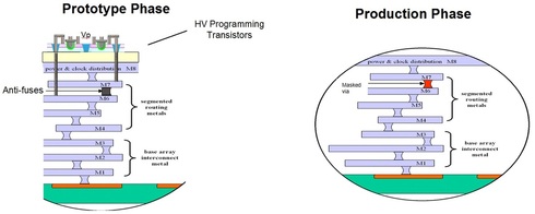
A special type of antifuse programmable technology could be most effective – Antifuse-based 3D High Density FPGA. This type of programmable fabric leverages anti-fuse metal to metal technology, which use 3D transistors for programming the anti-fuses. The 3D transistors could handle the higher voltage required for the programming and provide the interconnect programming with minimal device density impact. The 3D anti-fuse programmable fabric density is very similar to a via programmable fabric. Via programmable fabrics has been used with structured ASICs such as those offered by eASIC and Triad Semiconductors (ViASIC). They provide a programmable fabric with about a 2X area penalty vs. mask-defined standard cell technologies. These antifuses could be made as one time or reprogrammable devices and be fully replaced by mask-defined vias for even lower cost volume production, as illustrated by the following chart
Picture
Figure 8
Going forward, the semiconductor industry needs to go through fundamental change. No longer is it sufficient to scale using the next node of dimensional scaling to provide better overall device value. From the 28 nm node going forward, the industry needs to open up for a broad range of innovation so to continue offering better products. We can only hope that this will drive the industry back to fast growth and support the future market of Internet-of-Things and Internet-of-Everything.
submit to reddit
1 Comment

Why 450mm will be pushed-back even further

3/6/2014

0 Comments


A Must-See Chart from ISSCC2014

Picture
Zvi Or-Bach, MonolithIC 3D, & Ben Louie, Zeno Semiconductors

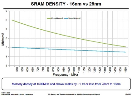
The chart below was presented at ISSCC 2014 by Dinesh Maheshwari, CTO of Memory Products Division at Cypress Semiconductors. The slide clearly illustrates that embedded SRAM ("eSRAM") scaling is broken. 
Picture
Instead of the expected 4X density improvement for a large memory block with two nodes of scaling, the improvement range is only 1.6X for low performance to 1.1X at good performance. Since eSRAM dominates most SoC silicon area, we have to conclude that dimensional scaling is broken as well. Let’s discuss it further.Instead of the expected 4X density improvement for a large memory block with two nodes of scaling, the improvement range is only 1.6X for low performance to 1.1X at good performance. Since eSRAM dominates most SoC silicon area, we have to conclude that dimensional scaling is broken as well. Let’s discuss it further.
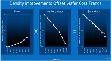
The following slide was presented by Intel at their recent analyst day. It illustrates the impact of dimensional scaling on advanced wafer cost ($/mm²) mostly due to the escalating cost of lithography. Intel believes it can compensate for this exponential wafer cost increase by increasing their transistor density (mm²/transistor) to maintain historical cost reduction of transistor cost ($/transistor).
Picture
Perhaps it can, but at this time we keep hearing about delays in ramping up the 14nm line. (See "Broadwell Coming, but Not Until the End of the Year.") This reminds us of the famous joke, "Will make it on the volume," since increasing transistor density is directly related to the aggressive dimensional scaling that was driving the escalating wafer cost in the first place.

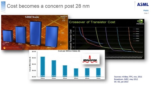
Most industry players confirm that cost-reduction for transistors has stopped beyond the 28nm process node, as is illustrated by the ASML chart below. This chart was presented at SEMICON West 2013.
Picture
It also clear that EUV is not going to be ready for the 16/14nm node. In fact, most observers are in agreement that EUV will also miss the 10nm node.

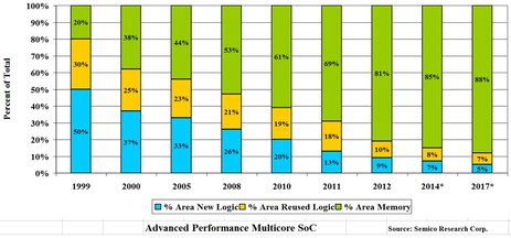
For some applications, keeping the cost-per-transistor about the same while reducing power or increasing speed might still justify going to 20nm or 14nm. The IMEC/Cypress chart above indicates that this will not be true for most designs. The fraction of the die area used for eSRAM is consistently growing with scaling, and it already regularly exceeds 50%. The following two charts from Semico, which were recently updated, illustrate this for advanced SoC and average SoC implementations.
Picture
Picture
Taking into account that 16/14 nm silicon is almost twice as expensive per unit area as that of 28 nm, this implies that beyond 28nm, SoC costs for the same functionality will escalate for most designs, and this will dampen even further the transition to advanced nodes such as 20nm or 16/14nm!

This clearly seems to indicate a paradigm shift after 50 years of consistent cost-reduction with dimensional scaling. Indications of this were already presented in our blog, Paradigm Shift: Semi Equipment Tells the Future, and in recent news articles such asAnalysis: ASML Stops 450mm Dead and Intel Cancels Fab 42.

Some people will attempt to brush aside Maheshwari's chart shown above, yet multiple sources indicate this is a true new reality that should not be ignored. We first reported it in our blog on ASML at Semicon West 2013, SRAM Scaling Has Stopped, which was backed up by the following IMEC chart as reported in Status Update on Logic and Memory Roadmaps.
Picture
This IMEC chart shows that the reduction of eSRAM bitcell area below 28nm is much less than the 50% expected size-reduction per technology node.

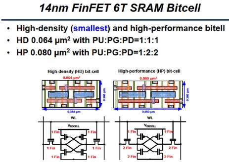
Furthermore, TSMC reported at IEDM 2013 that their bitcell for 16nm is 0.07µm2, and at ISSCC2014 Samsung presented similar results for 14nm finFETs as shown in the following slide.
Picture
It appears that the TSMC and Samsung bit cell sizes are in line with the IMEC table presented above. It also appears that these trends become even worse when comparing the size of high performance block RAM between technology nodes as presented by Maheshwari.

In the case of block RAM, additional aspects need to be taken into consideration, such as the die size impacts required for implementing a new technology such as finFET. In its ISSCC 2014 paper, Samsung identified complications involved with the transition from planar to finFET, such as quantized width, strong PMOS, and a lack of the body-bias effect. Samsung disclosed a die size impact of 0.87% in order to add a Disturbance Noise Reduction (DNR) scheme to deal with its larger, more stable High Performance (HP) bit-cell. Samsung did not disclose the area impact of its proposed Negative Bitline write assist scheme used with their high density HD bit-cell, but we can assume it is likely significantly larger than the proposed scheme for the HP bit-cell.

Some of the issues that are holding back scaling eSRAM were presented in our recent blog: The Most Expensive SRAM in the World -- 2.0. Bitcell scaling is getting harder, much harder, and even more so is the ability to scale large blocks of embedded SRAM. When we add the fact that the amount of embedded memory is growing faster than the amount of logic cells, one can predict dark clouds for SoC scaling beyond 28nm. It seems that brute-force scaling is simply not practical anymore, but two technology innovations could solve the SRAM memory scaling problem and provide a scalable high density memory if adopted soon by the industry.

The first innovation is the One-Transistor SRAM (1T SRAM) developed by Zeno Semiconductor. This 1T SRAM utilizes an existing fab process, provides a 90% bitcell size reduction versus conventional 6T SRAM, and it will keep scaling beyond 28nm. The second innovation is that of monolithic 3D, which enables a very effective heterogeneous integration scheme, thereby allowing for the SRAM layer to be optimized for memory while the logic layer can be optimized for logic. (See Monolithic 3D eDRAM on Logic.)

So, what do you think? Do you still believe that traditional scaling is the way to go? Or do you think that we will need to rely on new technologies like 1T-SRAM and monolithic 3D in order to maintain the pace of SoC development?
0 Comments
<<Previous

    Search Blog


    Meet the Bloggers


    Follow us


    To get email updates subscribe here:


    Recommended Links

    3D IC Community
    3D IC LinkedIn Discussion Group

    Recommended Blogs

    • 3D InCites by Francoise von Trapp
    • EDA360 Insider by Steve Leibson
    • Insights From the Leading Edge by Phil Garrou
    • SemiWiki by Daniel Nenni, Paul Mc Lellan, et al.

    Archives

    March 2022
    December 2021
    August 2021
    August 2018
    July 2018
    May 2018
    October 2017
    September 2017
    December 2016
    September 2016
    August 2016
    November 2015
    October 2015
    September 2015
    July 2015
    June 2015
    May 2015
    April 2015
    March 2015
    February 2015
    October 2014
    September 2014
    August 2014
    July 2014
    June 2014
    May 2014
    April 2014
    March 2014
    February 2014
    January 2014
    December 2013
    November 2013
    October 2013
    September 2013
    August 2013
    July 2013
    March 2013
    February 2013
    January 2013
    December 2012
    November 2012
    October 2012
    August 2012
    June 2012
    May 2012
    April 2012
    March 2012
    February 2012
    January 2012
    December 2011
    November 2011
    October 2011
    September 2011
    August 2011
    July 2011
    June 2011
    May 2011
    April 2011
    March 2011

    Categories

    All
    3d Design And Cad
    3dic
    3d Ic
    3d Nand
    3d Stacking
    3d Technology
    Brian Cronquist
    Dean Stevens
    Deepak Sekar
    Dram
    Education
    Heat Removal And Power Delivery
    Industry News
    Israel Beinglass
    Iulia Morariu
    Iulia Tomut
    Monolithic3d
    Monolithic 3d
    MonolithIC 3D Inc.
    Monolithic 3d Inc.
    Monolithic 3d Technology
    Moore Law
    Outsourcing
    Paul Lim
    Repair
    Sandisk
    Semiconductor
    Semiconductor Business
    Tsv
    Zeev Wurman
    Zvi Or Bach
    Zvi Or-Bach

    RSS Feed

© Copyright MonolithIC 3D Inc. , the Next-Generation 3D-IC Company, 2012 - All Rights Reserved, Patents Pending