Why Monolithic 3D?
The advanced technology patented by MonolithIC 3D
Inc. enables the fabrication of Monolithic 3D Integrated Circuits with multiple stacked transistor layers and ultra-dense vertical connectivity. For example, one could have 4 stacked transistor layers with vertical connections as small as 50nm. Building circuits with three dimensionally stacked transistors results in shorter wires, thereby tackling wire delay problems. Furthermore, stacked device layers increase the number of transistors per unit area without requiring costly feature size reduction. This, in turn, helps tackle cost issues with Dennard Scaling.
|
A number of studies have analyzed monolithic 3D-ICs from a theoretical perspective. Davis, et al. reported a 3x reduction in total silicon area and a 12x reduction in chip footprint for a monolithic 3D-IC with 4 device layers when compared to a 2D-IC [3]. The reduction in wire lengths enabled a size decrease of the logic gate drivers for these wires, which reduced the distance between logic gates (and wire length) further, causing a "positive feedback effect" that significantly reduced total silicon area. Synopsys reported that 3D-ICs could provide gains equivalent to 2 generations of Dennard scaling [4]. Zhou, et. al., reported a more than an order of magnitude improvement in the (power*area*delay) product for an LDPC decoder design [5].
|
What is the difference between Monolithic 3D and Through-Silicon Via (TSV) 3D technology starting to go to production? Follow this link to find out.
|
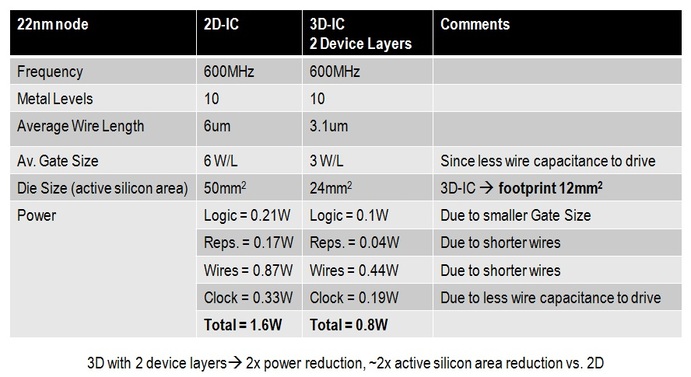
Figure 2: Comparison of a Monolithic 3D-IC and a 2D-IC at the same technology node.
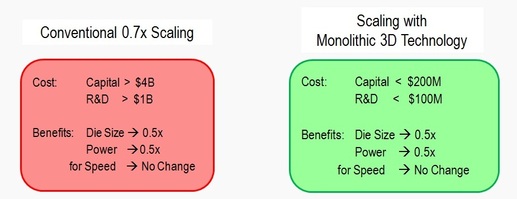
We analyzed the implications of Monolithic 3D technology using a 3D version of a CAD tool called IntSim [6].The study considered a 600MHz low-power 2D logic core constructed at the 22nm node as a baseline. Fig. 2 indicates that a monolithic 3D-IC with 2 device layers can provide a 2x reduction in power, a 2x reduction in total silicon area, and a 4x reduction in chip footprint (compared to a 2D-IC implementation). Thus, it appears monolithic 3D-ICs with 2 device layers provide benefits similar to a generation of conventional scaling. Furthermore, just as conventional scaling reduced feature sizes every generation, monolithic 3D opens the road for many years of continuous scaling by ‘folding’ once, twice, and so forth without necessarily reducing feature sizes. This could be particularly attractive since leading-edge fabs needed for conventional scaling today cost more than $5 billion and require more than $1 billion for process nodal R&D. With monolithic 3D type ‘folding’, the benefits of scaling can be achieved by utilizing predominantly the existing capital equipment and R&D. Estimates with Sematech's Cost-of-Ownership framework, combined with the results shown in Fig. 2, predict the data shown in Fig. 3. The monolithic 3D-IC seems to open a most compelling alternative to conventional scaling (for logic cores) due to its lower capital and R&D costs.
Figure 3: Cost estimates for Conventional Scaling and Monolithic 3D Scaling (for Logic Cores).
|
|
|


