Paths to Monolithic 3D
MonolithIC 3D Inc. offers multiple paths to silicon-based Monolithic 3D-ICs using building blocks well-known to the semiconductor industry. All these paths are patented or patent-pending and utilize a technique called ion-cut or
layer transfer, to get mono-crystalline silicon atop copper wiring at <400C. Ion-cut is the predominant
process used for manufacturing Silicon-on-Insulator (SOI) wafers today, and utilizes wafer-bonding [7]
and hydrogen-implant based cleave [8][9].
Path 1: Transistor Construction above Copper Interconnects at <400C
The first path to monolithic 3D-ICs involves sub-400C transistor construction above copper interconnect layers. Recessed ChAnnel Transistors (RCATs) [10] form a transistor family that can be constructed at <400C with our proposed procedures. RCATs have been used in DRAM manufacturing since the 90nm node [11]. We suggest using them for logic applications where Monolithic 3D is desired. Experimental data from DRAM manufacturers indicates that RCATs can have similar drive currents and significantly lower leakage when compared to planar transistors, at the cost of higher gate capacitance [10].
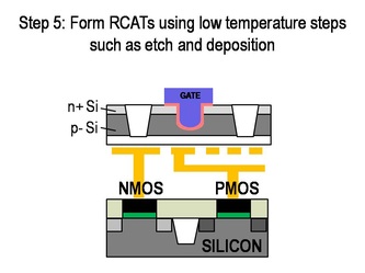
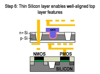
Figure 4: Simplified
Process Flow for Constructing RCATs atop Copper Interconnects.
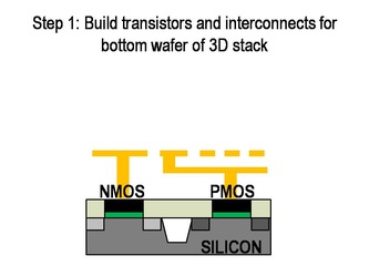
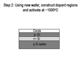
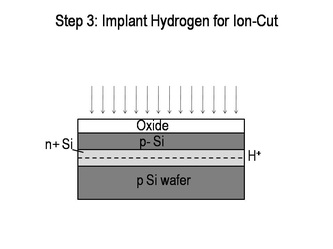
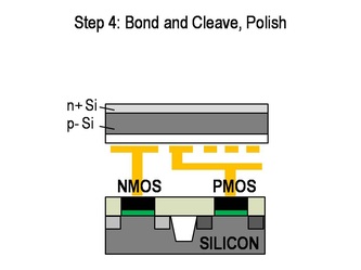
The procedure for construction of RCATs in 3D stacked layers is shown in Fig. 4.
Step 1: The bottom wafer of the 3D stack having transistors and copper interconnects is conventionally built.
Step 2: A bilayer stack of p- Si and n+ Si on a new wafer is constructed using implant and epitaxial processes. The dopants are activated with normal high-temperature techniques.
Step 3: Hydrogen is implanted into the wafer with p- and n+ Si regions, which creates a plane of defects at the desired depth within the wafer.
Step 4: The wafer shown in Step 3 is flipped and oxide-to-oxide bonded atop the structure shown in Step 1. The structure is then cleaved at the hydrogen plane using either a mechanical force [8] or a sub-400C anneal [9], leaving the thin doped layers of mono-crystalline silicon atop the bottom wafer.
Step 5: Recessed ChAnnel Transistors (RCATs) are formed using etch, deposition and other processes typically conducted at <400C. The gate dielectric and gate electrode are deposited with Atomic Layer Deposition (ALD).
Step 6: Interconnects (intra-layer and inter-layer) are processed with standard BEOL resolution and alignment, enabled by the thin (tens to low hundreds of nm) top device layer.
The process flow shown above has three unique characteristics:
(1) Process steps for transistors that require >400C, such as implant activation, are conducted before layer transfer. This ensures compatibility with bottom wafer copper interconnects.
(2) Recessed channel transistors, that allow a transistor to be defined with sub-400C processes such as etch and deposition, are used.
(3) Layer to layer interconnect for the 3D stack is accomplished at close to full lithographic resolution and alignment.
Path
2: State-of-the-Art Replacement-Gate Transistor Stacking
A second path to monolithic 3D-ICs constructs the stack with any state-of-the-art transistor that uses a replacement-gate process. Innovative alignment schemes, combined with repeating layouts, help obtain sub-50nm, and hence dense, through-silicon electrical connections.
A second path to monolithic 3D-ICs constructs the stack with any state-of-the-art transistor that uses a replacement-gate process. Innovative alignment schemes, combined with repeating layouts, help obtain sub-50nm, and hence dense, through-silicon electrical connections.
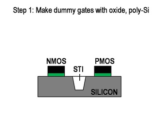
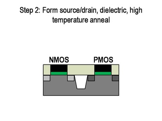
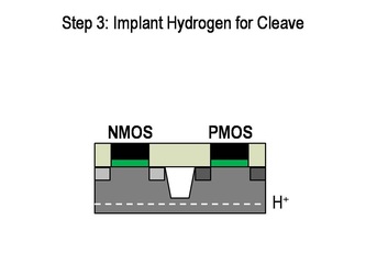
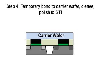
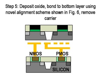
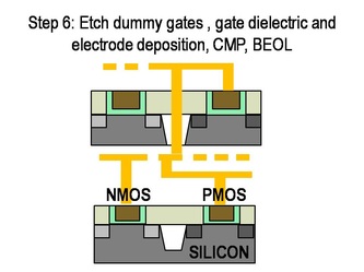
Figure 5: Simplified Process Flow for State-of-the-Art Replacement-Gate Transistor 3D Stacking.
Fig. 5 describes the process flow.
Step 1: Transistor regions are constructed with gate dielectrics and dummy gates.
Step 2: Source-drain regions are formed normally with high temperature processing.
Step 3: Hydrogen is implanted at the desired depth for ion-cut purposes.
Step 4: The wafer is face-up bonded to a temporary carrier wafer, then cleaved at its hydrogen plane, and then the exposed backside is polished.
Step 5: The wafer backside surface is coated with oxide and bonded to the bottom wafer having pre-processed transistors and interconnects. A novel alignment scheme, described in Fig. 6, is used to obtain well-aligned sub-50nm through-silicon connections. After bonding, the carrier wafer is removed.
Step 6: The state-of-the-art replacement-gate process [12] proceeds normally (remove and replace dummy gates) and standard BEOL ensues with intra-layer and inter-layer interconnect formation as shown. Note: This process sequence prevents degradation of device characteristics due to implant damage to the silicon dioxide gate dielectric in Step 3.
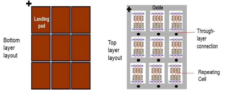
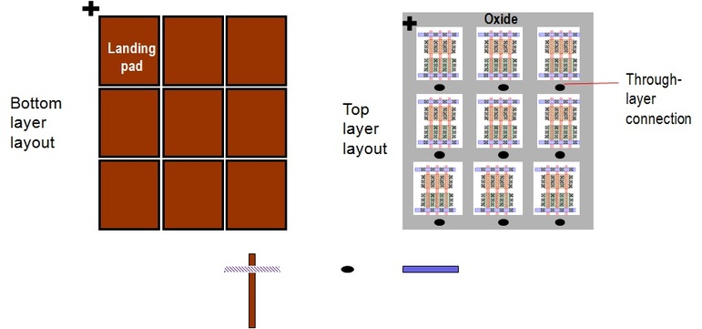
The novel alignment scheme used in Fig. 5 (Step 5) is described at a high-level with Fig. 6. Fig. 6(a) shows the layout of the bottom layer of the 3D stack and Fig. 6(b) shows the layout of the top layer of the 3D stack. The top layer of devices has a repeating layout, similar to a gate array. Many companies are moving to similar layouts due to lithographic limitations. The bottom layer has landing pads, which are structures around the same size as each repeating cell. Even if misalignment occurs during bonding, since the top layer is a set of repeating cells, the desired top layer circuitry will still be connected to any specific landing pad. This misalignment tolerance scheme enables a high density of through-layer connections. The key advantage of this scheme is it’s applicability to any state-of-the-art transistor constructed with a replacement gate process. The alignment scheme that we expect to implement commercially is more sophisticated and area-efficient than the one explained with Fig. 6, and is described in US Patent Application 12/847,911 (summarized in Fig. 7 for convenience).
(a) (b)
Figure 6: Repeating layout structures used to tackle wafer bonding misalignment for the (a) bottom layer and (b) top layer of the 3D stack.
Figure 6: Repeating layout structures used to tackle wafer bonding misalignment for the (a) bottom layer and (b) top layer of the 3D stack.
Fig. 7: A more sophisticated alignment scheme where the brown vertical track exists on the bottom wafer and the blue horizontal track exists on the top wafer. The via in between has X alignment done to the bottom wafer's alignment mark and Y alignment done to the top wafer's alignment mark.
|
|
|

