Monolithic 3D Inc., the Next Generation 3D-IC Company
  • Home
  • Technology
    • Technology
    • Papers, Presentations and Patents
    • Overview >
      • Background
      • Why Monolithic 3D?
      • Paths to Monolithic 3D
      • Applications
    • Ion-Cut: The Building Block
    • Monolithic 3D Logic >
      • RCAT
      • HKMG
      • Laser Annealing
      • RCJLT
      • 3D Embedded RAM
      • 3D Gate Array
      • FPGA
      • Ultra Large Integration - Redundancy and Repair
    • Monolithic 3D Memory >
      • 3D DRAM
      • 3D Resistive Memories
      • 3D Flash
    • Monolithic 3D Electro-Optics >
      • 3D Image Sensors
      • 3D Micro-Displays
  • 3D-IC Edge
    • 3D-IC Edge
  • News & Events
    • News & Events
    • S3S15 Game Change 2.0 Video/P
    • Webcast
    • Webinar
    • Press Releases
    • In the News
    • Upcoming Events
  • About Us
    • About Us
    • History
    • Team
    • Careers
    • Contact Us
  • Blog
  • Simulators

Is Tech Heading to a Recession?

3/14/2015

0 Comments

 
Picture
We have a guest contribution from Zvi Or-Bach, the President and CEO of MonolithIC 3D Inc. 
Moore’s law has swept much of the modern world along with it. Some estimates ascribe up to 40 percent of the global productivity growth achieved during the last two decades to the expansion of information and communication technologies made possible by semiconductor performance and cost improvements... 

"Samsung and smartphones in general look to be in trouble and that's bad news for the electronics industry" wrote Rick Merritt in his Smartphone, Samsung in Trouble recent report from MWC15 in Barcelona. Rick clearly points to 14nm FinFET as the source of the problem and continues  "[i]f smartphone growth slows for lack of a driver, as tablet growth is already doing, the electronics industry could be in trouble ... it’s beginning to feel like another big bubble building up."

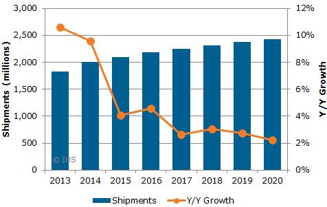
Few days later, the following chart supporting Rick’s impression was released in a new report from IHS. 
Picture
Source: IHS Quarterly Mobile Phone Display Shipment and Forecast Report
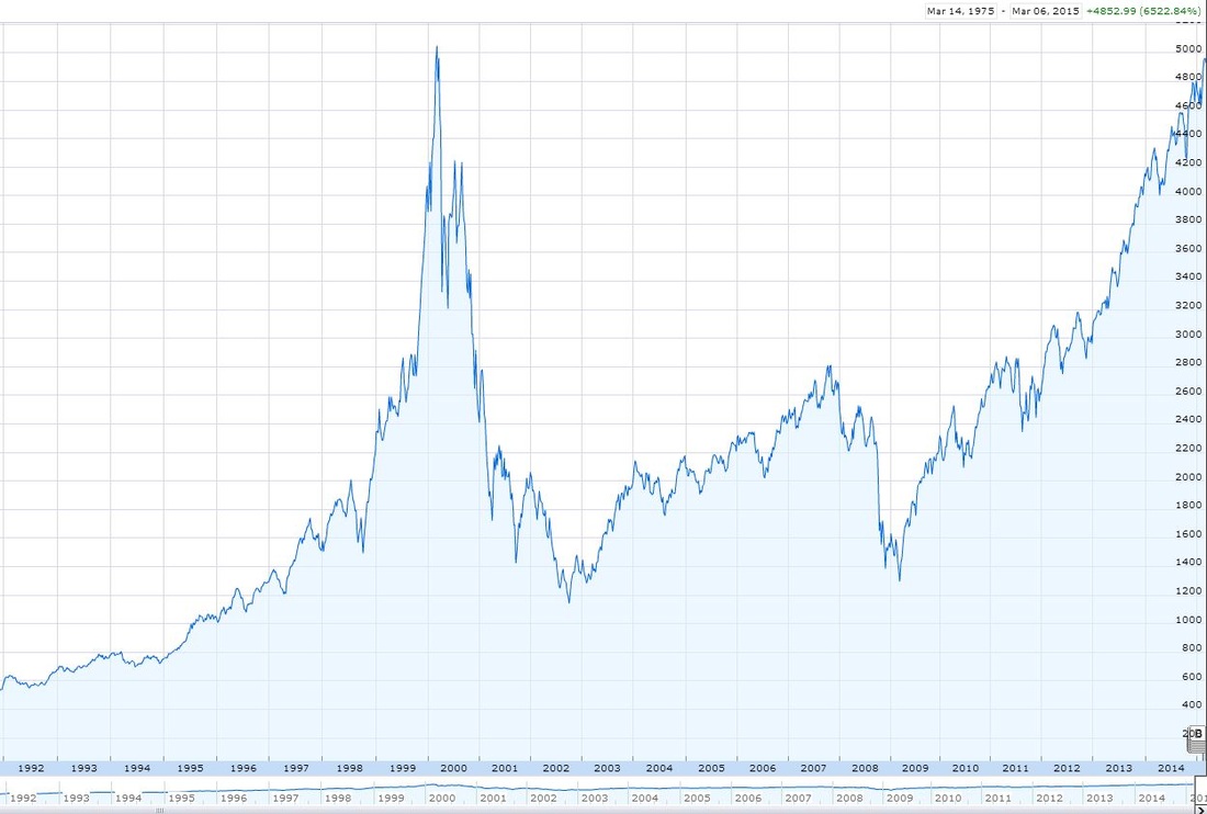
All this comes just as NASDAQ seems to finally be reaching back to the height of the Tech Bubble seen in the following chart:
Picture
About a year ago McKinsey published a report Moore’s law: Repeal or renewal? subtitled "Economic conditions could invalidate Moore’s law after decades as the semiconductor industry’s innovation touchstone. The impact on chipmakers and others could be dramatic." It goes on to say
As a result, Moore’s law has swept much of the modern world along with it. Some estimates ascribe up to 40 percent of the global productivity growth achieved during the last two decades to the expansion of information and communication technologies made possible by semiconductor performance and cost improvements... The law retains its predictive power because of constant improvements in production technology, which are driven by the industry’s “global semiconductor road maps.” These describe the progress required for the continuation of Moore’s law.

The report concludes with this: "We believe that interesting years lay ahead for the semiconductor industry because the steady evolution the industry historically counted on might be coming to an end."

And it does seem that this is ahead of us as we presented in our well-read blog 28nm: The Last Node of Moore's Law.

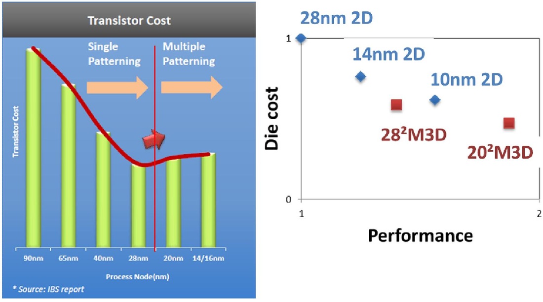
Since the publication of that blog more information has been released, mostly supporting the conclusion that 28 nm was the last node. This includes the following finding from a survey conducted by KPMG "Only a fourth of semiconductor business leaders believe Moore's Law will continue for the foreseeable future ... More than half said Moore’s Law will no longer apply at various nodes less than 22 nanometers, while 16 percent said it already has ended." Similarly,  Scott McGregor, President and CEO of Broadcom, spoke at SEMI Industry Strategy Symposium (ISS) in January (Exponentially Rising Costs Will Bring Changes) and indicated that the cost per transistor was rising after the 28nm, which he described as “one of the most significant challenges we as an industry have faced.” He provided the following slide in support:
Picture
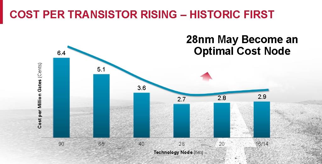
"The reason for increasing transistor cost is the complexity of the devices, and the cost of the equipment required to produce them. … these costs are going up exponentially," he said.

The good news is that we now have an alternative, scaling up using monolithic 3D. As was presented in last year’s IEEE S3S-2014 conference and in our blog - Precision Bonders - A Game Changer for Monolithic 3D, monolithic 3D IC could be adopted by any current fab without the need for a new recipe for transistor formation, providing very competitive costs for a wide range of product enhancements and offers a long-term road map for the industry. 
submit to reddit
0 Comments

Intel Calls for 3D IC

3/5/2015

0 Comments

 
Picture
We have a guest contribution from Zvi Or-Bach, the President and CEO of MonolithIC 3D Inc.

At the recent ISSCC Intel presented the following slide. Quoting from Extremetech coverage: "At 10nm and below, the path forward will become increasingly murky. What Intel has proposed is essentially a shift towards other types of cost-saving technologies and process adoptions rather than relying on strict lithography improvement … Intel may be keeping its next-generation materials and lithography plans quiet, but the company does intend to push the envelope in other ways. 2.5D and 3D integration will be critical to the development of next-generation SoCs"
Picture
We clearly agree with Intel that the heterogeneous integration enabled by 3D IC is an "increasingly important part of scaling". This will become even more true as mobile and IoT markets increasingly will consume the lion share of the semiconductor business.

With respect to "Poor for Low Cost," this is only true for the TSV approach to 3D ICs. The following slide was presented in the recent 3D ASIP (2014) conference as the summary of "Will the Cost of 3D ICs Ever Be Low Enough for High Volume Products" presentation by Chest Palesko, a leading market researcher:
Picture
So, yes TSV-based 3D IC is "Poor for Low Cost".

But the other form of 3D IC, the Monolithic 3D, is the lowest cost path for future scaling!

Samsung’s 3D NAND is an early example of monolithic 3D enabled scaling, being driven primarily by the push to increase bit capacity while reducing the cost per bit. Monolithically scaling up is now part of the ITRS and is being adopted by all NAND vendors. Samsung was the first to bring 3D NAND to mass production using the monolithic 3D approach:
Picture
Picture
The next market segment adopting monolithic 3D scaling is the image sensors as recently reported by EE Times: CMOS Image Sensors Surpassing Moore's Law. Quoting: "imaging chips is downsizing the chip while simultaneously packing more pixels per unit size, thus one-upping processors and memory … The CMOS imaging industry may make the 3-D TSV obsolete – before the processor and memory industry has even widely adopted it – by perfecting a wafer bonding technique that allows the connection between layers to be made with copper-to-copper (Cu-to-Cu) interconnects nearly as small as regular vias."

While still in the R&D phase, there is momentum building for monolithic 3D in logic too, as reported by CEA Leti’s work in collaboration with ST Micro, IBM, and Qualcomm. This was presented in the S3S (2014), 3D ASIP (2014), and IEDM (2014) conferences. The following chart was presented by CEA Leti and shows the cost reduction and performance improvements enabled by monolithic 3D scaling:
Picture
Figure 5: Cost vs performance opportunities for Monolithic 3D integration. By stacking older generations M3DI allows containing the cost increase associated to double patterning introduction
A recent validation of the unreasonable costs associated with dimensional scaling beyond 28 nm could be calculated from a recent EE Times article TSMC to Start 10nm in 2017, Closing Gap with Intel. Quoting: "By the end of 2018, the company’s Taichung site will reach a monthly output capacity of 90,000 wafers at the 10nm and more advanced technology nodes, according to a report on the Chinatimes.com website. TSMC earlier this month said it would invest NT$500 billion ($15.9 billion) as part of an expansion at the Taichung site in central Taiwan." At two year’s depreciation, this represents $7,400 per wafer!!!

A misleading benefit which often gets attributed to dimensional scaling but has little to do with it, is the wide range of device improvements resulting from R&D efforts that typically coincide with the next scaling node. AMD’s recent presentation at ISSCC 2015 clearly illustrates this point by showing device improvements while still staying at the same 28 nm process node. As could be seen, major improvement in power, yield, and performance are possible over time without changing the technology node.
Picture
Picture
Monolithic 3D provides the industry many years of exponential integration growth while reducing cost and power by leveraging depreciation, learning curve, heterogeneous integration, low VT, SOI, shorter interconnections and many other powerful benefits of monolithic 3D, some of which are presented in our white paper The Monolithic 3D Advantage, monolithic 3D is far more than just an alternative to 0.7x scaling!!!

Until recently, the path to monolithic 3D required change to the front end-of-line process. An FEOL process change is always part of dimensional scaling, but is expensive, risky and in most cases done only by the leading edge companies. Now, as was presented in the recent IEEE S3S ‘14 conference, emerging precision bonders, such as from EVG or Nikon, enable a Game Changer for Monolithic 3D  - a "true monolithic 3D IC without the need for a new recipe for transistor formation. The process could be adopted by any current fab providing very competitive costs for a range of product enhancements and offers a long term road map for better offerings by scaling up."


P.S.

A good conference to learn about this new scaling technology is the IEEE S3S ‘15, in Sonoma, on October 5th thru 8th, 2015. Two leading researchers from Berkeley and Stanford Universities will give invited talks presenting their work on advanced monolithic 3D integration technologies.
submit to reddit
0 Comments

    Search Blog


    Meet the Bloggers


    Follow us


    To get email updates subscribe here:


    Recommended Links

    3D IC Community
    3D IC LinkedIn Discussion Group

    Recommended Blogs

    • 3D InCites by Francoise von Trapp
    • EDA360 Insider by Steve Leibson
    • Insights From the Leading Edge by Phil Garrou
    • SemiWiki by Daniel Nenni, Paul Mc Lellan, et al.

    Archives

    March 2022
    December 2021
    August 2021
    August 2018
    July 2018
    May 2018
    October 2017
    September 2017
    December 2016
    September 2016
    August 2016
    November 2015
    October 2015
    September 2015
    July 2015
    June 2015
    May 2015
    April 2015
    March 2015
    February 2015
    October 2014
    September 2014
    August 2014
    July 2014
    June 2014
    May 2014
    April 2014
    March 2014
    February 2014
    January 2014
    December 2013
    November 2013
    October 2013
    September 2013
    August 2013
    July 2013
    March 2013
    February 2013
    January 2013
    December 2012
    November 2012
    October 2012
    August 2012
    June 2012
    May 2012
    April 2012
    March 2012
    February 2012
    January 2012
    December 2011
    November 2011
    October 2011
    September 2011
    August 2011
    July 2011
    June 2011
    May 2011
    April 2011
    March 2011

    Categories

    All
    3d Design And Cad
    3dic
    3d Ic
    3d Nand
    3d Stacking
    3d Technology
    Brian Cronquist
    Dean Stevens
    Deepak Sekar
    Dram
    Education
    Heat Removal And Power Delivery
    Industry News
    Israel Beinglass
    Iulia Morariu
    Iulia Tomut
    Monolithic3d
    Monolithic 3d
    MonolithIC 3D Inc.
    Monolithic 3d Inc.
    Monolithic 3d Technology
    Moore Law
    Outsourcing
    Paul Lim
    Repair
    Sandisk
    Semiconductor
    Semiconductor Business
    Tsv
    Zeev Wurman
    Zvi Or Bach
    Zvi Or-Bach

    RSS Feed

© Copyright MonolithIC 3D Inc. , the Next-Generation 3D-IC Company, 2012 - All Rights Reserved, Patents Pending