
We have a guest contribution from Zvi Or-Bach, the President and CEO of MonolithIC 3D Inc. Zvi discusses The Pivotal Point for Monolithic 3D IC.
From our biased point of view we see the recent IEDM12 as a pivotal point for monolithic 3D. Here’s why:
We start with the EE Times article IEDM goes deep on 3-D circuits, starting with "Continuing on the theme of 3-D circuit technology addressed in an earlier post about this year’s International Electron Device Meeting, Rambus, Stanford University and an interesting company called Monolithic 3D will address issues related to cooling 3-D circuits. .." and follow with a quote from the abstract to IEDMs short course "Emerging Technologies for post 14nm CMOS" organized by Wilfried Haensch, of IBM’s Watson Research Center:
We start with the EE Times article IEDM goes deep on 3-D circuits, starting with "Continuing on the theme of 3-D circuit technology addressed in an earlier post about this year’s International Electron Device Meeting, Rambus, Stanford University and an interesting company called Monolithic 3D will address issues related to cooling 3-D circuits. .." and follow with a quote from the abstract to IEDMs short course "Emerging Technologies for post 14nm CMOS" organized by Wilfried Haensch, of IBM’s Watson Research Center:
"Scaling the dimension was the key for the unprecedented success of the development of IC circuits for the last several decades. It now becomes apparent that scaling will become increasingly difficult due to fundamental physical limits that we are approaching with respect to power and performance trade-offs. This short course will give an overview of several aspects in this “end-of-scaling” scenario. ..."
We then continue with statements made by Dr. Howard Ko, a Senior Vice President and General Manager of the Silicon Engineering Group of Synopsys in his 2013: Next-generation 3-D NAND flash technology article:
"Yet there are a variety of developments in another type of 3-D scaling that are likely to have a similarly large impact on semiconductors in the near future - 3-D devices for NAND flash.... And as in planar CMOS logic, NAND flash technology has been progressively scaled to smaller feature sizes, becoming the process leader in driving the smallest line-widths in manufacturing as evidenced by the current 1x-nm (~19-nm) process node. Yet, despite plans to scale down to the 1y-nm (~15-nm) and possibly 1z-nm (~13-nm) nodes, the traditional planar floating gate NAND flash architecture is approaching the scaling limit, prompting the search for new device architectures. Not to be upstaged by the planar to 3-D (FinFET) transition in logic devices, NAND flash has embarked on its own 3-D scaling program, whereby the stacking of bit cells allows continuous cost-per-bit scaling while relaxing the lateral feature size scaling."
In our recent blog 3D NAND Opens the Door for Monolithic 3D we discussed in detail the adoption of monolithic 3D for the next generations of NAND Flash. The trend was very popular subject of this year’s IEDM and is nicely illustrated by this older chart:
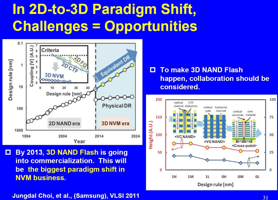
Figure 1
And accordingly the updated ITRS 2012 present the change from dimension scaling to monolithic 3D scaling as presented in the following slide.
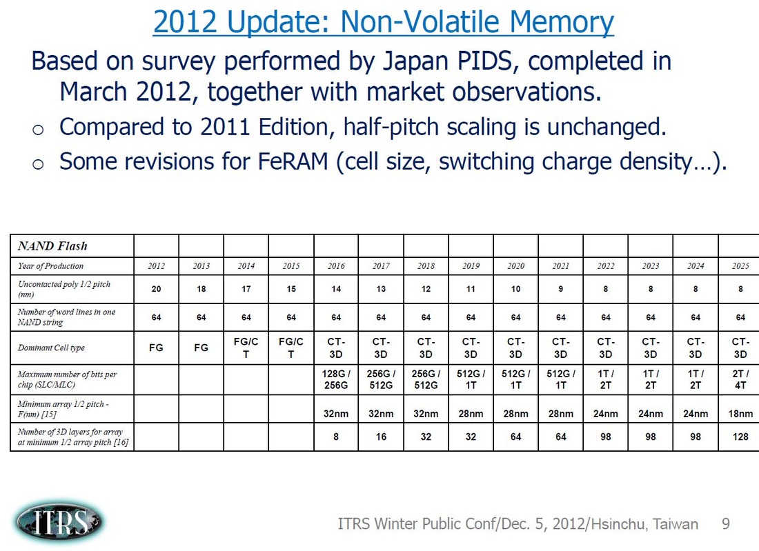
Figure 2
This year’s IEDM brought up two of the driving forces behind the shift from dimensional scaling to monolithic 3D IC scaling, that we will detail below as #1 and #2.
The Current 2D-IC is Facing Escalating Challenges:
The problem with on-chip interconnect didn’t start today. This vintage Synopsys slide below clearly indicates that on-chip interconnect started to dominate overall device performance a decade ago:
The Current 2D-IC is Facing Escalating Challenges:
- On-chip interconnect (#1)
- Dominates device power consumption
- Dominates device performance
- Penalizes device size and cost
- Lithography (#2)
- Dominates Fab cost
- Dominates device cost and diminishes scaling benefits
- Dominates device yield
- Dominates IC development costs
The problem with on-chip interconnect didn’t start today. This vintage Synopsys slide below clearly indicates that on-chip interconnect started to dominate overall device performance a decade ago:
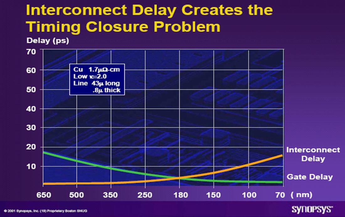
Figure 3
In response, the industry has spent an enormous amount of money to convert from aluminum to copper and to low-K inter-metal dielectrics. But now, we have very few additional options left (perhaps air-bridge?) as illustrated by the following chart:

Figure 4
It shows that neither Carbon Nano Tube (CNT) nor Optical interconnect are better than copper, and that monolithic 3D still is the best path.
The practiced ‘band-aid’ fix so far has been throwing more transistors (they are getting cheaper, right? No longer. See father below) at the problem in the form of buffer and repeaters. But as we scale down we need exponentially more of these ban-aids as illustrated by the following:
The practiced ‘band-aid’ fix so far has been throwing more transistors (they are getting cheaper, right? No longer. See father below) at the problem in the form of buffer and repeaters. But as we scale down we need exponentially more of these ban-aids as illustrated by the following:
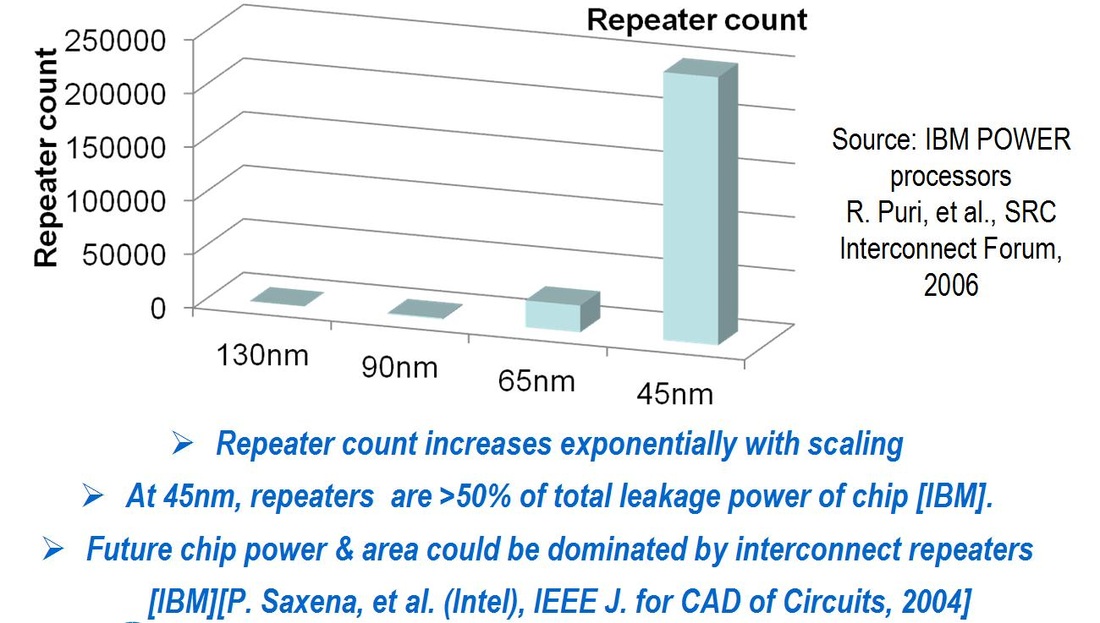
Figure 5
Copper, however, is now reaching its inflection point as was articulated in a special session organized by Applied Materials attached to this IEDM, The 14 nanometer node is expected to be an inflection point. Quoting from the abstract:
"The 14 nanometer node is expected to be an inflection point for the chip industry, beyond which the resistivity of copper interconnects will increase exponentially and may become a limiting factor in chip design. On December 11, 2012, Applied Materials, Inc. will host an important forum in San Francisco to explore the path that interconnect technology must take to keep pace with transistor scaling and the transition to new 3D architectures.” (emphasis added)
This had been illustrated before in the following chart
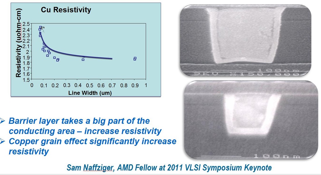
Figure 6
And to make it crystal clear, IBM presented the following chart in its short course:
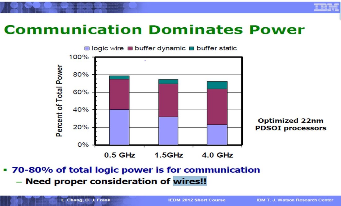
Figure 7
Power is now dominating IC design and clearly dimensional scaling does not improve the interconnect’s impact – see the following chart built from the ITRS Roadmap. The only effective path forward that addresses interconnect is monolithic 3D.
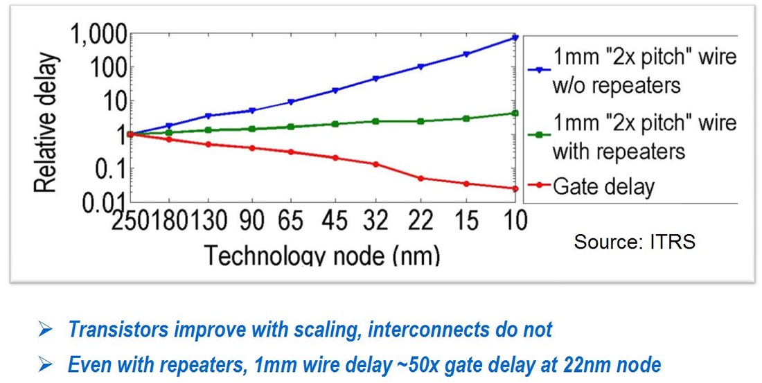
Figure 8
As for the second challenge – lithography – we start again with an old chart by Synopsys:
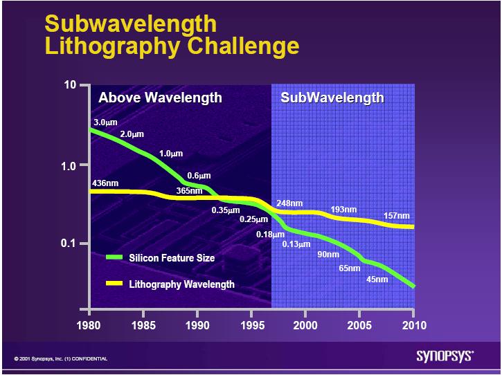
Figure 9
The implication is that any new node of dimensional scaling comes with escalating lithography costs; and sure enough, that’s what is happening. When litho costs are plotted over time, it fits a log-linear scale….this is not a sustainable trend.
The following chart illustrate the lithography escalating cost of equipment which directly reflect the wafer cost.
The following chart illustrate the lithography escalating cost of equipment which directly reflect the wafer cost.
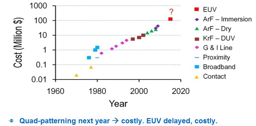
Figure 10
This resulted in the following slide by IBM at the GSA Silicon Summit 2012:
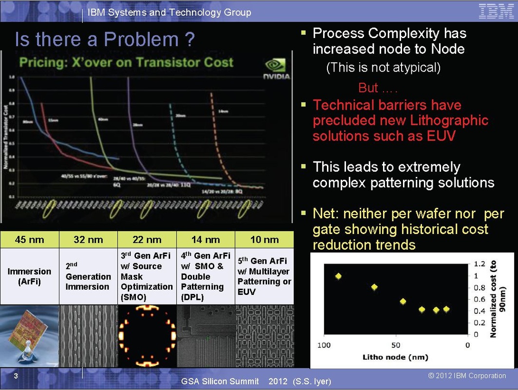
Figure 11
Quoting from the slide: "Net: neither per wafer nor per gate [are] showing historical cost reduction trends"
Another EE Times IEDM12 article covering a keynote given by Luc van den Hove, chief executive of IMEC, IEDM: Moore’s Law seen hitting big bump at 14 nm, repeats the same conclusion. In fact, some vendors are already changing course accordingly. GlobalFoundries, in its recent 14nm announcement, disclosed that the back-end will be unchanged from 20nm. This suggests a similar die size and respective increase in per-transistor cost. Further, ST Micro in the Fully Depleted Transistors Technology Symposium (11 December, 2012) during IEDM12 week also acknowledged that their 14nm node will have a 20nm node metal pitch, and, just like GlobalFoundries, a similar die size and increase in per-transistor cost. So it would seem that also for lithographic reasons, the industry’s next generation path, and the continuation of Moore's Law, would be achieved by leveraging the third dimension.
Now that monolithic 3D is feasible and practical, the time has come to move in this new direction, as has been nicely illustrated by this concluding chart below
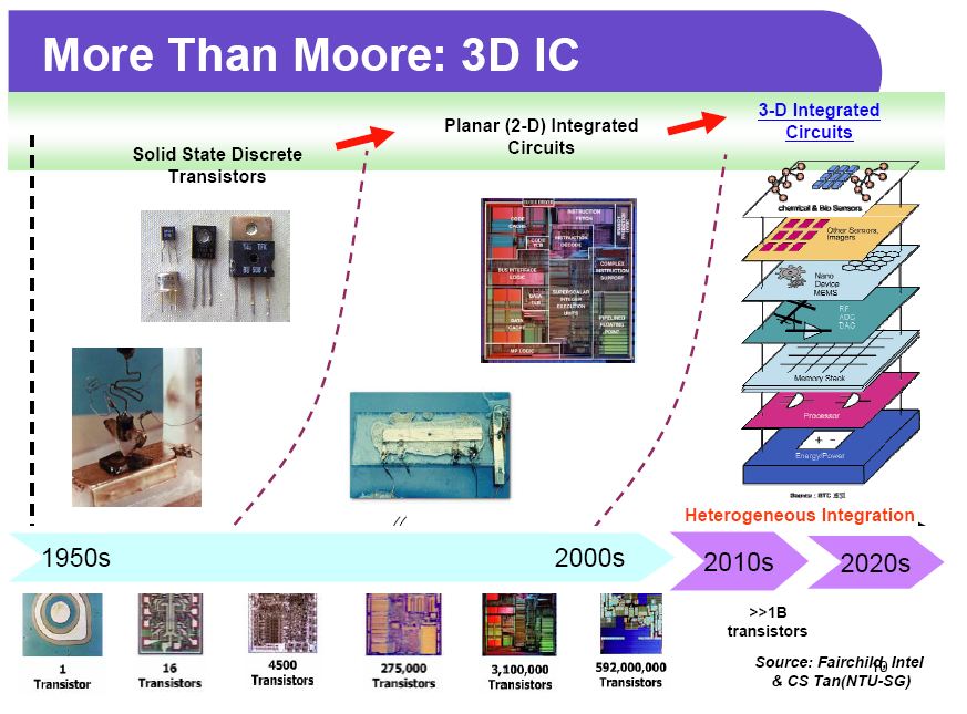
Figure 12


 RSS Feed