
We have a guest contribution from Zvi Or-Bach, the President and CEO of MonolithIC 3D Inc. Mr. Or-Bach discusses about the latest news shared by Qualcomm.
"Qualcomm is looking to monolithic 3D and smart circuit architectures to make up for the loss of traditional 2D process scaling as wafer costs for advanced nodes continue to increase." Speaking in a keynote at DAC 2014 in San Francisco, vice president of engineering Karim Arabi, is reported to argue that 3D and EDA need to make up for Moore’s Law.This was the third time in the past year that Qualcomm executives have made such a call at major industry conferences. At IEDM 2013 Geoffrey Yeap, Qualcomm VP of Technology, stated in his invited talk: "As performance mismatch between transistors and interconnects continue to increase, designs have become interconnect-limited. Monolithic 3D (M3D) is an emerging integration technology poised to reduce the gap significantly between transistors and interconnect delays to extend the semiconductor roadmap way beyond the 2D scaling trajectory predicted by Moore’s Law." Yeap provided the following chart for the growing gap between transistor delay and interconnect delay

Figure 1
Earlier that year, Robert Gilmore, Qualcomm VP Engineering, in his invited talk at VLSI 2013 (Kyoto, Japan), used almost the same words and provided the following illustration (note the wafer is face-down):
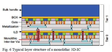
Figure 2
Clearly there seems to be a concentrated effort by Qualcomm to promote the development and adoption of monolithic 3D.
Qualcomm has done more than just talking. It has been investing in monolithic 3D development tools with institutions such as Georgia Tech (see their GTCAD LAB website reporting technology transfer in 2012 and 2014). Qualcomm has been filing patents in this area and recently announced an agreement to work with CEA-Leti - Qualcomm to Evaluate Leti’s Non-TSV 3D Process
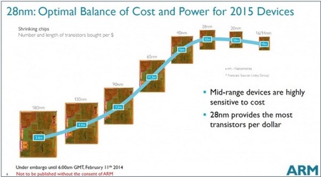
It would seem that the number one motivation behind these efforts is Qualcomm’s concern about future cost reductions. Early in 2012 Jim Clifford, Qualcomm's VP and GM (at that time), in his plenary talk at the SPIE conference titled - A Mobile Wireless Phenomenon: A Continued Need for Advanced Lithography, made it very clear with his second slide. At that time there were already some concerns with EUV’s rollout schedule. Jim called on the conference attendees to make sure to solve the escalation of advanced lithography cost, which was already dominating more than 50 % of the overall advanced device cost. Jim presented the following curve, showing the historical 29% cost reduction per year, and the looming problem with the production cost beyond 28 nm.
Qualcomm has done more than just talking. It has been investing in monolithic 3D development tools with institutions such as Georgia Tech (see their GTCAD LAB website reporting technology transfer in 2012 and 2014). Qualcomm has been filing patents in this area and recently announced an agreement to work with CEA-Leti - Qualcomm to Evaluate Leti’s Non-TSV 3D Process
It would seem that the number one motivation behind these efforts is Qualcomm’s concern about future cost reductions. Early in 2012 Jim Clifford, Qualcomm's VP and GM (at that time), in his plenary talk at the SPIE conference titled - A Mobile Wireless Phenomenon: A Continued Need for Advanced Lithography, made it very clear with his second slide. At that time there were already some concerns with EUV’s rollout schedule. Jim called on the conference attendees to make sure to solve the escalation of advanced lithography cost, which was already dominating more than 50 % of the overall advanced device cost. Jim presented the following curve, showing the historical 29% cost reduction per year, and the looming problem with the production cost beyond 28 nm.
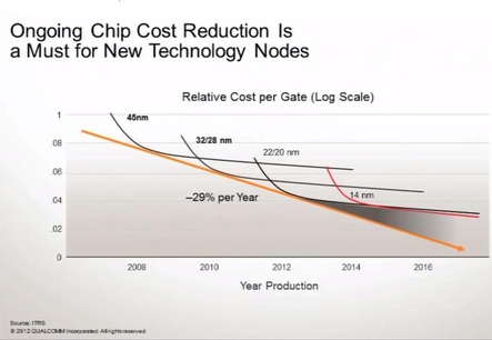
Figure 3
Jim than said: "If the next node doesn't cost less than the last node we got a problem because I don't think the demand will be there." Well it is now clear that EUV is not ready and that dimensional scaling below 28nm will require double and triple lithography with its associated extra costs.
Back to the DAC 2014 keynote: Arabi explained: “Mobile is becoming a centre of gravity for the user. It is providing a unique opportunity ... but it becomes a challenge to develop because you have to integrate them at lower power and low cost as well ... One of the biggest problems is cost. We are very cost sensitive. Moore’s Law has been great. Now, although we are still scaling down, it’s not cost-economic anymore. It’s creating a big problem for us.” As we reported in our recent blog, 28nm – The Last Node of Moore's Law, dimensional scaling below 28 nm will result in increasing device cost. This was echoed multiple times at this DAC by other keynote speakers such as Hossein Yassaie, CEO of Imagination Technologies, who said: “Moore’s Law is really over from my point of view. It’s not that it can’t scale, it’s that the cost is not going down anymore".
Back to the DAC 2014 keynote: Arabi explained: “Mobile is becoming a centre of gravity for the user. It is providing a unique opportunity ... but it becomes a challenge to develop because you have to integrate them at lower power and low cost as well ... One of the biggest problems is cost. We are very cost sensitive. Moore’s Law has been great. Now, although we are still scaling down, it’s not cost-economic anymore. It’s creating a big problem for us.” As we reported in our recent blog, 28nm – The Last Node of Moore's Law, dimensional scaling below 28 nm will result in increasing device cost. This was echoed multiple times at this DAC by other keynote speakers such as Hossein Yassaie, CEO of Imagination Technologies, who said: “Moore’s Law is really over from my point of view. It’s not that it can’t scale, it’s that the cost is not going down anymore".
Figure 4
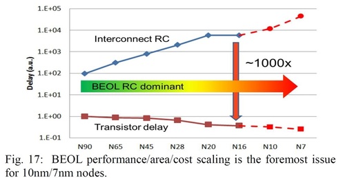
And cost is not the only problem with dimensional scaling. The following IBM slide illustrates that interconnect now dominates device power.
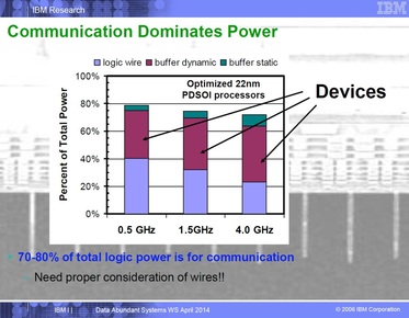
Figure 5
Interconnect’s effect on power is just getting worse with dimensional scaling. Arabi also stated in his DAC keynote: “Interconnect RC is inching up as we go to deeper technology. That is a major problem because designs are becoming interconnect-dominated. Something has to be done about interconnect. What needs to be done is monolithic three-dimensional ICs ... So we are looking at true monolithic 3D. You have normal vias between different stacks. Then interconnect lengths will be smaller than with 2D. If we can connect between layers the delay becomes smaller. This is a technology for the end of the decade, but it can give us an advantage of one process node, with a 30 per cent power saving and a 40 per cent gain in performance.”
Clearly, monolithic 3D integration has a very important role for the future of the semiconductor industry. It is therefore fitting that the traditional IEEE conference on SOI has extended its scope and now calls itself S3S: SOI technology, 3D Integration, and Subthreshold Microelectronics. The 2014 S3S conference is scheduled for October 6-9, 2014 at the Westin San Francisco Airport. This would be a great opportunity to learn more about monolithic 3D technology with 5 invited presentations covering topics from design tools to monolithic 3D NAND and other 3D memories, CEA Leti will present their work on CMOS monolithic 3D IC, and researchers from MIT and Stanford will present manufacturing monolithic 3D devices with materials other than silicon.
Clearly, monolithic 3D integration has a very important role for the future of the semiconductor industry. It is therefore fitting that the traditional IEEE conference on SOI has extended its scope and now calls itself S3S: SOI technology, 3D Integration, and Subthreshold Microelectronics. The 2014 S3S conference is scheduled for October 6-9, 2014 at the Westin San Francisco Airport. This would be a great opportunity to learn more about monolithic 3D technology with 5 invited presentations covering topics from design tools to monolithic 3D NAND and other 3D memories, CEA Leti will present their work on CMOS monolithic 3D IC, and researchers from MIT and Stanford will present manufacturing monolithic 3D devices with materials other than silicon.


 RSS Feed