Monolithic 3D Inc., the Next Generation 3D-IC Company
  • Home
  • Technology
    • Technology
    • Papers, Presentations and Patents
    • Overview >
      • Background
      • Why Monolithic 3D?
      • Paths to Monolithic 3D
      • Applications
    • Ion-Cut: The Building Block
    • Monolithic 3D Logic >
      • RCAT
      • HKMG
      • Laser Annealing
      • RCJLT
      • 3D Embedded RAM
      • 3D Gate Array
      • FPGA
      • Ultra Large Integration - Redundancy and Repair
    • Monolithic 3D Memory >
      • 3D DRAM
      • 3D Resistive Memories
      • 3D Flash
    • Monolithic 3D Electro-Optics >
      • 3D Image Sensors
      • 3D Micro-Displays
  • 3D-IC Edge
    • 3D-IC Edge
  • News & Events
    • News & Events
    • S3S15 Game Change 2.0 Video/P
    • Webcast
    • Webinar
    • Press Releases
    • In the News
    • Upcoming Events
  • About Us
    • About Us
    • History
    • Team
    • Careers
    • Contact Us
  • Blog
  • Simulators

Who Will Be the Winners?

10/29/2012

0 Comments

 
Picture
We have a guest contribution today from Ze'ev Wurman, MonolithIC 3D Inc.'s Chief Software Architect. Ze'ev discusses about where is the semiconductor industry heading to.

The semiconductor industry is in the doldrums. The PC market shrinks, Intel shares sink, Applied Materials cuts staff, and even Apple suddenly experiences its share price drop by $100 in a month. Are things really so bad?

But other news seems different. TSMC shares are close to their historical high; Global Foundries leapfrogs TSMC technology and nips at Intel’s heels with 14nm; Samsung reports record quarterly profit. Things seem to be going swimmingly.

Semiconductor business has had its ups and downs since its inception. As demand followed, more and more capacity was put on line, which caused the next overcapacity and slump, inevitably followed by the next spike in demand as the technology inexorably marched down the scaling curve. So, perhaps, nothing is really new here after all.

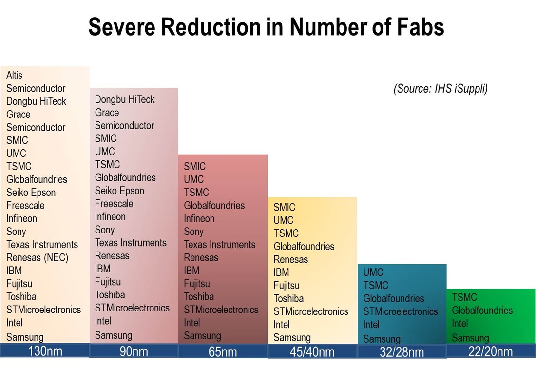
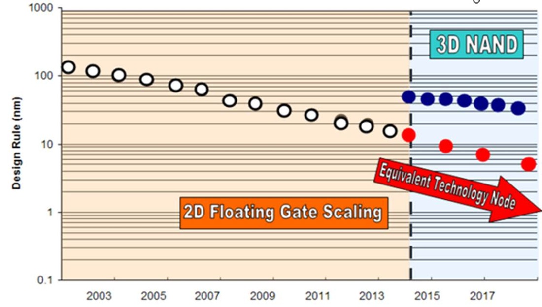
Yet, perhaps, we should not be so sanguine anymore. We did cope with 193nm light to define our chips down to 20 nm, but at an ever-increasing cost of expensive phase shift masks, immersion lithography, and double exposure. EUV has been talked about for at least 15 years (following another 15 years of x-ray lithography development fiasco) and has been “late” since at least 2005. Despite the impressive progress shown by ASML, the industry greats – Intel, Samsung, and TSMC --banding around EUV is possibly more a sign of desperation than a strong vote of confidence. The drastic reduction in foundry players – from 20 or so in 90nm to four or less for 14nm has been noticed by many and cannot be good for the long-term health and vitality of the industry. 
Picture
ASML is the last remaining game in town and, even if it works, building a foundry at over $10B a pop, and developing a technology node at well north of $1B, does wonders at keeping everyone but the most committed (and with deep pockets) out of the game. And the unanswered question is still in place: at what price point will the industry effectively become the domain of the few mass-produced designs such as Apple’s or Samsung’s phones and nothing else? 
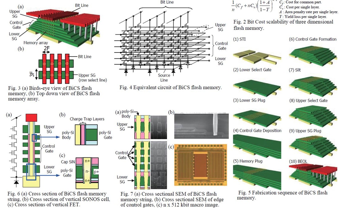
Picture
Figure 2
Clearly pressures have been building up and the industry can’t pretend everything is as usual for much longer.  3D devices has been talked about for decades, yet implementing this dream was considered infeasible until recently. 3D designs are, in a sense, the holy grail of the industry:

  • They allow for shrinkage of the average source to destination distances, shrinking power dissipation and improving performance;
Picture
  • They can include inexpensive built-in fault detection and repair as described here, allowing for as large as needed yielded dies, which cuts further on power by saving on off-chip I/O power;
  • They allow cheap and high performance integration of dies with disparate technologies, so advanced (and expensive)  logic can be stacked with reduced-cost technology for memory dies, or specialized analog and RF functions;
  • They allow the reuse of older fab lines as much of density improvement is achieved through stacking dies rather than shrinking features;
Picture
  • They allow efficient heat removal without exotic cooling technologies through use of power delivery networks, to be presented in the upcoming IEDM, paper 14.2 ;
In recent years TSVs started to show up. Yet, while TSVs are good for designs that need limited vertical connectivity between disparate sub-systems such as processors with memory, they do not really open the door to a true monolithic 3D design.  What true monolithic devices offer is a much higher vertical connectivity, by a factor of up to 10,000, and enable the stacking of multiple dies.

The impact of the increased monolithic vertical integration at lower cost can be dramatic on every electronic market segment.

For mobile devices, the inexpensive integration of analog, RF, and sensors, can lower their cost and power consumption for an even broader market penetration and longer battery life.

In medicine, the footprint of devices is often critical. The availability of camera-in-a-pill, or of implantable medical devices that control drug release, improve hearing, monitor vital signs, or allow artificial vision, are all strongly dependent on heterogeneous device integration in a small footprint and with reduced power. Monolithic 3D is key to transforming the planar and bulky designs of today’s 2D to grain-of-corn and grain-of-rice shape factors that can be inserted for very long time periods into our bodies.

Fostering innovation and reducing barriers to entry of new products are considered crucial for future economic prosperity. FPGAs have been trying to fill this niche since the demise of ASICs, yet they suffer from many handicaps: they are physically large, they are power hungry, and they are available in a limited number of configurations that are often suboptimal for the application. Monolithic 3D technology allows the inexpensive creation of a nearly infinite number of FPGA configurations that can be tailored to every application, as described here. And it does so while dramatically reducing both the device footprint and power.

Large-scale computing is facing enormous challenges to reduce its power consumption. Server farms of the likes of Google, Amazon, or Facebook consume tens and hundreds of megawatts of energy, while the government struggles mightily to keep its planned Exascale supercomputer under 20MW. Three-dimensional chips can play a large role in reducing power consumption by reducing the interconnect length (and hence, its capacitance), which is responsible for most of the power dissipation in modern chips. Ultra large scale integration with high yields, enabled through 3D repair structures, will further slash the power that today resides in the off-chip drivers.

In memory design, the transition to 3D technology is already taking place as described in our previous blog. Monolithic 3D structures using crystalline silicon may further the penetration and efficacy of this technology in both non-volatile memory as well as in DRAM.

The semiconductor world will inevitably move to monolithic three-dimensional technologies. The change drivers are already here: the skyrocketing cost of scaled-down lithography, the need to reduce power dissipation, and the need for heterogeneous integration. The only question is how quickly it will move there, and who will be the winners.
submit to reddit
0 Comments

3D NAND Opens the Door for Monolithic 3D

10/1/2012

2 Comments

 
Picture
We have a guest contribution today from Israel Beinglass, the CTO of MonolithIC 3D Inc. Israel discusses the opportunities of 3D NAND with Monolithic 3D.

NAND technology, which is a subset of NVM (Non Volatile Memory), was invented by Fujio Masuoka of Toshiba back in 1984. Flash memory was presented at IEDM1984 by Dr. Masuoka and his colleagues [1].  The following is a short quote from the original paper “the cell is programmed by a channel hot carrier injection mechanism similar to EPROM. The contents of all memory cells are simultaneously erased by using field emission of electrons from a floating gate to an erased gate in a FLASH (Hence the name FLASH)”.  

Masuoka came back to the IEDM in 1987 and suggested a Flash NAND structure [2].
Intel created the first commercial NOR type of Flash chips in 1988. For the next few years some major developments occur in the Flash arena:
  • In 1989, Samsung and Toshiba created a NAND flash memory.
  • In 1994, Compact Flash was invented and introduced by SanDisk.
  • In 1999, the SD memory card was released by a combination of SanDisk, Toshiba and Matsushita.
  • In 2001, the world’s first 1 Gigabit Compact Flash card was introduced.
From 2006 onwards, NAND became the most scaled of devices beating out the microprocessor devices (see Figure 1). The current state of the art is 20nm (2x) technology, as the world’s appetite for storage is still strong. Flash Cards, SSD, Smartphone and Tablets are the leading growing applications.
Picture
Figure 1: Flash Vs. Microprocessor design rules cross over
NAND memory as a true cross point array with the control gate on top of the floating gate and only one contact for a whole string of cells has the smallest memory cell size as shown in Figure 2 In addition, when one adds with the capability of MLC (Multi Level Cells) to NAND devices, the bit density dramatically increases.
Picture
Figure 2: NAND, circuit diagram and SEM pictures in x and y directions.
The NAND market has been continuously growing for the last several years. Figure 3 shows the NAND revenue and Gigabytes increase since 2008 and the forward projection for the years 2012-2016.
Picture
Figure 3: NAND Revenue and Gigabytes growth
As the NAND technology has been moving to smaller and smaller process nodes some serious problems, physical and electrical surfaced:
           Physical Limitations:
  • Pattern scaling - lack of EUV is a major issue
  • Structure formation, Figure 4 depicts a 27nm NAND cell that shows how close the cells are getting to each other, and how much the aspect ratio is getting out of hand. This is a limiter to obtaining high yield.
          Electrical Limitations:
  • There is an increase in cell-to-cell interference in the word lines.
  • Capacitive coupling ratio has decreased
  • Dielectric leakage has increased
The number of electrons on the floating gate has decreased dramatically so much so that a small fluctuation in the number on the floating gate can make a huge effect on the cell function. Figure 5 describes the scaling induced phenomenon.
Picture
Figure 4: A 27nm NAND cell structure
Picture
Figure 5: Number of electrons on the FG decreases for advanced NAND technology nodes
It is a common understanding among the experts that the current NAND technology will not be able to be scaled down to the 10nm node.

The solution for this dilemma is the 3D NAND, which was initially proposed by Toshiba at the 2007 VLSI Symposium [3]. Toshiba unveiled its Bit Cost Scalable (BiCS) technology. BiCS makes use of a “punch-and plug” structure and charge trap memory films. Toshiba has fabricated a prototype 32-Gbit BiCS flash memory test array with a 16-layer memory cell using 60nm design rules, see Figure 6. Hynix, Samsung and Macronix have also come with their versions of the 3D NAND.
Picture
Figure 6: 3D NAND process steps, as described by Toshiba
The following are the key advantages of the 3D NAND:

  • With 3D NAND, scaling is no longer driven by lithography. The gate length is defined by deposition
  • The key steps to 3D NAND are
                                        - Build a multitude of oxide/nitride or oxide/doped polysilicon stacked layers
                                - Fill the deep memory holes or trench slits. The top foreseeable challenges are ultra-high-aspect ratio (>40:1) conductor etch and dielectric etch with high etch selectivity to the hard mask
  • 3D NAND is relatively straightforward for a DRAM maker since it has stacked SiO2 and polysilicon layers like a stacked capacitor DRAM, and trenches like a trench cell DRAM. 
  • 3D NAND is evolutionary, not revolutionary. 
  • The good news is continued cost reduction, smaller die sizes and more capacity. 
  • Installed NAND toolsets in the wafer Fabs can, for the most part, be reused, thereby extending the useful life of Fab equipment. 
  • 3D NAND technology is still basically NAND with all its inherent limitations of data reliability and performance: hence, generally well understood (evolutionary).
At this point all the NAND companies are putting a lot of effort to bring this process to high volume manufacturing; the current expectations are that in 2014-2015 it will be ready for prime time. 3D NAND will be a technology that will take us between the 2D planar NAND and whichever post-NAND technology emerges in the future.
Picture
Figure 7: 3D NAND effect on design rules
Figure 7 describes the essence of the advantage of moving from 2D to 3D NAND. The adoption of 3D NAND technology will remove the burden from the Litho (and hence EUV) into the much easier process steps (deposition). Of course there are other advantages as described above.

It is not too difficult to see the similarity between the up and coming 3D NAND and the Monolithic 3D approach. As we describe in our web site (www.monolithic3d.com) the advanced technology patented by MonolithIC 3D Inc. enables the fabrication of Monolithic 3D Integrated Circuits with multiple stacked transistor layers and ultra-dense vertical connectivity. Thus, it appears monolithic 3D-ICs with 2 device layers provide benefits similar to a generation of conventional scaling. Furthermore, just as conventional scaling reduces feature sizes every generation, monolithic 3D opens the road for many years of continuous scaling by ‘folding’ once, twice, and so forth without necessarily reducing feature sizes.


  1. F. Masuoka et. al IEDM 1984 pp464-467
  2. F. Masuoka et. al IEDM 1987 pp552-555
  3. H. Tanaka et al., Symp. on VLSI Tech. Dig., pp 14-15, 2007
submit to reddit
2 Comments

    Search Blog


    Meet the Bloggers


    Follow us


    To get email updates subscribe here:


    Recommended Links

    3D IC Community
    3D IC LinkedIn Discussion Group

    Recommended Blogs

    • 3D InCites by Francoise von Trapp
    • EDA360 Insider by Steve Leibson
    • Insights From the Leading Edge by Phil Garrou
    • SemiWiki by Daniel Nenni, Paul Mc Lellan, et al.

    Archives

    March 2022
    December 2021
    August 2021
    August 2018
    July 2018
    May 2018
    October 2017
    September 2017
    December 2016
    September 2016
    August 2016
    November 2015
    October 2015
    September 2015
    July 2015
    June 2015
    May 2015
    April 2015
    March 2015
    February 2015
    October 2014
    September 2014
    August 2014
    July 2014
    June 2014
    May 2014
    April 2014
    March 2014
    February 2014
    January 2014
    December 2013
    November 2013
    October 2013
    September 2013
    August 2013
    July 2013
    March 2013
    February 2013
    January 2013
    December 2012
    November 2012
    October 2012
    August 2012
    June 2012
    May 2012
    April 2012
    March 2012
    February 2012
    January 2012
    December 2011
    November 2011
    October 2011
    September 2011
    August 2011
    July 2011
    June 2011
    May 2011
    April 2011
    March 2011

    Categories

    All
    3d Design And Cad
    3dic
    3d Ic
    3d Nand
    3d Stacking
    3d Technology
    Brian Cronquist
    Dean Stevens
    Deepak Sekar
    Dram
    Education
    Heat Removal And Power Delivery
    Industry News
    Israel Beinglass
    Iulia Morariu
    Iulia Tomut
    Monolithic3d
    Monolithic 3d
    MonolithIC 3D Inc.
    Monolithic 3d Inc.
    Monolithic 3d Technology
    Moore Law
    Outsourcing
    Paul Lim
    Repair
    Sandisk
    Semiconductor
    Semiconductor Business
    Tsv
    Zeev Wurman
    Zvi Or Bach
    Zvi Or-Bach

    RSS Feed

© Copyright MonolithIC 3D Inc. , the Next-Generation 3D-IC Company, 2012 - All Rights Reserved, Patents Pending