MonolithIic 3D RCAT
Monolithic 3D RCAT
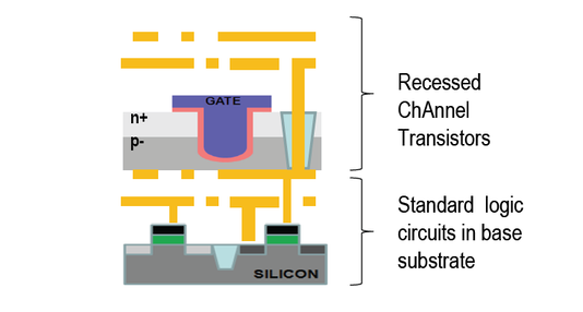
TechnologyThe monolithic 3D IC technology is applied to producing monolithically stacked low leakage Recessed ChAnnel Transistors (RCATs), commonly used in DRAM chips since the 90nm node.
Experimental data from DRAM manufacturers indicates that RCATs can have similar drive currents and significantly lower leakage when compared to planar transistors, at the cost of higher gate capacitance. Monolithic 3D IC provides a path to reduce logic, SOC, and memory costs without investing in expensive scaling down. |
Benefits
|
Process flow
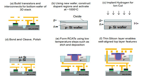
Create a layer of Recessed ChAnnel Transistors (RCATs), commonly used in DRAMs, by activating dopants at ~1000C before wafer bonding to the CMOS substrate and cleaving, thereby leaving a very thin dopant stack layer from which transistors are completed, utilizing less than 400C etch and deposition processes.
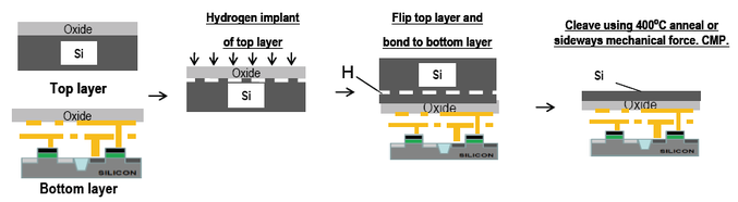
Layer Transfer Technology (“Ion-Cut”)Defect-free single crystal obtained @ <400C
Leveraging a mature technology (wafer bonding and ion-cleaving) that has been the dominant SOI wafer
production method for over two decades.
production method for over two decades.
Innovate and create multiple thin (10s – 100s nanometer scale) layers of virtually defect free Silicon by utilizing low temperature (<400C) bond and cleave techniques, and place on top of active transistor circuitry. Benefit from a rich layer-to-layer interconnection density.