Scaling will keep on using 28/22 nm
|
We have a guest contribution from Zvi Or-Bach, the President and CEO of MonolithIC 3D Inc.
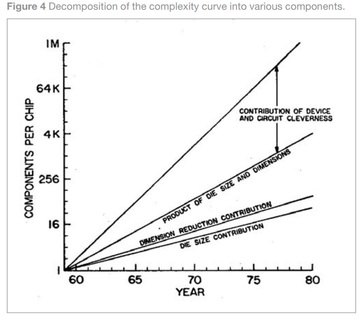
In his famous 1965 paper Cramming more components onto integrated circuits, Moore wrote: “The complexity for minimum component costs has increased at a rate of roughly a factor of two per year”. Dimensional scaling below 28nm will only increase the ‘component cost’ as described in 28nm – The Last Node of Moore's Law. |
1. “Die size”—“larger chip area”
2. “Dimension”—“higher density” and “finer geometries”
3. “Device and circuit cleverness”
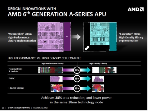
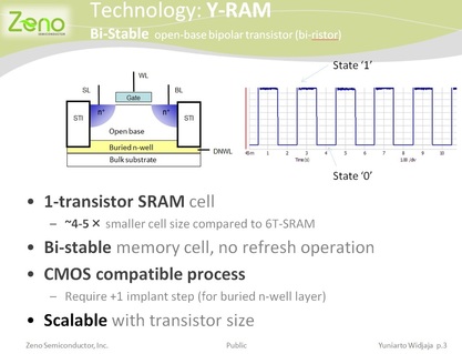
In the past, all of these factors were aggregated into dimensional scaling as old fabs got obsolete and improvements predominantly were implemented in the new emerging node. Nowadays, as dimensional scaling has reached its diminishing returns phase, we can see a very diverse adaption of technology improvments.
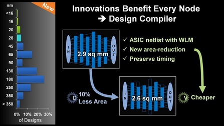
In his keynote presentation at the 2014 Synopsys user group meeting, Art De Geus, Synopsys CEO, presented multiple slides to illustrate the value of Synopsys’ newer tools to improve older node design effectiveness. The following is one of them
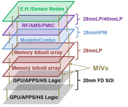
Finally, I’d like to quote Mark Bohr again as we reported in our blog “Intel Calls for 3D IC”: “heterogeneous integration enabled by 3D IC is an increasingly important part of scaling". This is illustrated nicely by the following figure presented by Qualcomm in their ISPD ‘15 paper titled “3D VLSI: A Scalable Integration Beyond 2D”
P.S.
A good conference to learn about these new scaling technologies is the IEEE S3S ‘15, in Sonoma, CA, on October 5th thru 8th, 2015. CEA Leti is scheduled to give an update on their CoolCube program and three leading researchers from Berkeley, Stanford and Taiwan’s NLA Lab will present their work on advanced monolithic 3D integration technologies.




 RSS Feed