Monolithic 3D Inc., the Next Generation 3D-IC Company
  • Home
  • Technology
    • Technology
    • Papers, Presentations and Patents
    • Overview >
      • Background
      • Why Monolithic 3D?
      • Paths to Monolithic 3D
      • Applications
    • Ion-Cut: The Building Block
    • Monolithic 3D Logic >
      • RCAT
      • HKMG
      • Laser Annealing
      • RCJLT
      • 3D Embedded RAM
      • 3D Gate Array
      • FPGA
      • Ultra Large Integration - Redundancy and Repair
    • Monolithic 3D Memory >
      • 3D DRAM
      • 3D Resistive Memories
      • 3D Flash
    • Monolithic 3D Electro-Optics >
      • 3D Image Sensors
      • 3D Micro-Displays
  • 3D-IC Edge
    • 3D-IC Edge
  • News & Events
    • News & Events
    • S3S15 Game Change 2.0 Video/P
    • Webcast
    • Webinar
    • Press Releases
    • In the News
    • Upcoming Events
  • About Us
    • About Us
    • History
    • Team
    • Careers
    • Contact Us
  • Blog
  • Simulators

Why Samsung will give Morris Chang sleepless nights

2/5/2012

13 Comments

 
Samsung contributes just 7% to the world’s foundry revenue today. But here’s why it could be TSMC’s biggest challenge yet...

Most people will agree that Andy Grove has been the semiconductor industry's most successful CEO. After co-founding Intel and serving as COO for many years, he took over the CEO role and oversaw a 2400% increase in the company’s stock price. Among the present set of semiconductor CEOs, does anyone possess Grove’s high levels of performance, dynamism and vision? There can be only one answer: Morris Chang, the founder and CEO of TSMC.

I’m sure many of you have read Andy Grove’s classic book, “Only the Paranoid Survive”. Let’s now apply the principles in Grove’s book to the foundry industry. If you were Morris Chang and had 50% market share in the foundry industry, which competitor of yours would you be “paranoid” about?

Picture
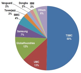
Figure 1: Foundry Revenue in 2011 (Source: SemiMD).

Fig. 1 shows the foundry landscape at the end of 2011. Many competitors show up: there’s Globalfoundries with its plentiful oil money, UMC with its excellent customer service and high yields and SMIC with its Chinese government backing. But, to me, Samsung is undoubtedly the biggest threat to TSMC, even though its foundry market share today is just 7%. Let me explain why...

Economies of Scale due to Memory Business

Semiconductor manufacturing costs are heavily dependent on economies of scale. Fig. 2 [1][2], which is an estimate of DRAM costs and selling prices in 2003, illustrates this point. The highest volume producer, Samsung, has the lowest raw material costs in Fig. 2. The same goes for semiconductor equipment purchases. A higher volume producer gets a lower price per tool. You’ll notice the highest volume producer (Samsung) has the lowest depreciation cost in Fig. 2.
Picture
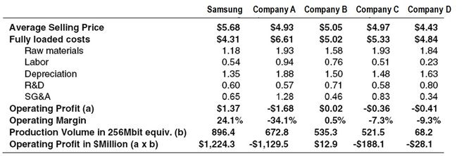
Figure 2: DRAM industry landscape in 2003. Costs are a function of production volumes. (Source: [1][2])

What does this mean for the foundry industry? Well, TSMC, since it has 50% market share, should benefit from economies of scale and build a lead over its rivals, right? That certainly gives TSMC an advantage over UMC and Globalfoundries, but doesn’t work with Samsung. Why? Because Samsung owns a huge chunk of the world’s memory business (~40%). It buys tools and raw materials in huge volumes for those markets, and you use pretty similar tools and raw materials for logic foundry manufacturing. Fig. 3 illustrates that Samsung’s capital expenditure for tools in 2012 is actually double that of TSMC. Samsung might therefore have lower raw material costs and depreciation costs than TSMC.

Picture
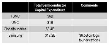
Figure 3: Samsung buys more semiconductor equipment than TSMC (numbers shown for 2012). Scale of equipment buying provides low prices. (Source: SemiMD)

Yield improvement methodologies

Samsung has a great set of yield improvement methodologies developed over its years in the competitive memory industry. Fig. 5 [2] illustrates yields of different DRAM manufacturers in 2003. You’ll notice Samsung has, by far, the best yields. Based on this data and Samsung’s reputation for high-yield memory products, you would expect Samsung to get good yields in the logic foundry business.  They seem to be delivering on that front. I hear from industry contacts that Samsung is the only manufacturer getting reasonable yields for gate-first high k metal gate products at 28nm.
Picture
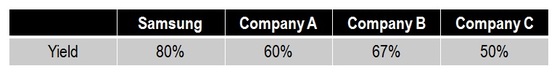
Figure 4: Samsung’s yield enhancement methodologies gave it an advantage over competitors in the memory industry. (Source: [2])

Low cost fabs

In cost sensitive markets such as memory and foundries, the location of a fab makes a difference. Fig. 5 [3] shows a chart from the US National Academy of Engineering which reveals that fab costs in the US are ~25% higher than fab costs in the Far East. Some of TSMC’s competitors have fabs in Europe and the US, but Samsung is building a good portion of its capacity in Korea (they do have one facility in Texas though). The fab cost advantage TSMC has over its other competitors doesn’t necessarily exist with Samsung.
Picture
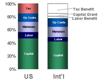
Figure 5: Cost of US fabs higher than those in Korea, Taiwan or Singapore. (Source: [3])

Sensible partnership strategy

One of the barriers to entry for the foundry business is availability of Intellectual property (IP) blocks and CAD tool support. Intel, which is looking to enter the foundry business, has difficulties with this, since IP blocks haven’t been developed for its technologies yet. SoC makers today show a marked preference for foundries offering competitive IP blocks at low prices.

When Samsung entered the foundry industry, it addressed this issue by joining the IBM alliance, and so its customers could use IP blocks developed for the IBM alliance. Samsung did not have much experience developing logic technologies either, and the alliance helped Samsung learn from existing players in the logic business such as IBM and Globalfoundries. In spite of having a similar technology offering to Globalfoundries and IBM, Samsung retains an advantage over these competitors since it is better at ramping up yields and because it has low cost fabs.

R&D costs for next-generation logic technologies are $1-2 billion today. Sharing the cost with IBM and Globalfoundries gives Samsung a R&D cost advantage over companies such as TSMC and UMC which develop new technologies alone.

Ability to fund large capital expenditures

TSMC, UMC, Globalfoundries and SMIC derive almost all their sales from the foundry industry. This limits the amount of capacity they can add every year, since their balance sheets place restrictions on maximum cap-ex to revenue ratio (Globalfoundries is an exception here due to its oil money). Samsung, on the other hand, is a diversified company that sells everything from TVs to DRAM to NAND flash to cell phones. It routinely takes profits from other divisions and invests it in the logic foundry industry. Fig. 6 [4] illustrates this trend. Samsung’s capex to revenue ratio for its foundry business is way higher than anyone else. This added capacity is helping Samsung’s foundry business grow rapidly  – notice how Samsung’s froundry revenues increased almost 7x between 2010 and 2012. Samsung used this “capacity-add-like-there-is-no-tomorrow” strategy to become our industry’s biggest DRAM producer, so the foundry folks had better watch out!
Picture
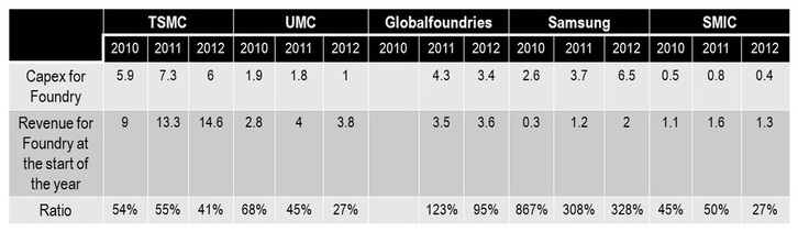
 Figure 6: Samsung has the highest cap-ex to revenue ratio among all foundries. (Source: SemiMD)

Proven Research Expertise

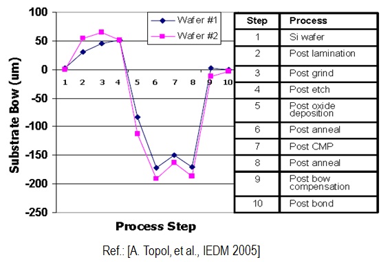
If you talk with engineering folks in our industry and ask them which companies do the best research, you will find Samsung near the top of the list. Let me illustrate Samsung’s research capabilities using Monolithic 3D as an example. They started working on the technology almost 10 years back, and have developed monolithic 3D technologies for NAND flash, SRAM and resistive memories. In addition, their roadmap calls for commercialization of Monolithic 3D NAND flash memories within 2 years. Check out Fig. 7. This is some of the best work I’ve seen on monolithic 3D so far. This phenomenal research capability will help Samsung make strides in the logic space.
Picture
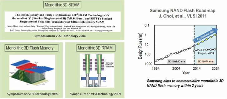
Figure 7: Samsung has a long history of developing monolithic 3D technologies.

Caveat

While the above capabilities of Samsung threaten TSMC in the long term, there are stormy clouds looming for Samsung in the short term. Apple, which accounts for more than 75% of Samsung’s foundry revenues [4] today, is flirting with TSMC due to its increasingly litigious competition with Samsung in the mobile space. If TSMC executes well and takes this business away from Samsung, it could be a big blow to Samsung’s ambitions.

To summarize

I explained why I believe Morris Chang will consider Samsung his biggest competitor in the long-term. The economies of scale Samsung has due to its memory business could help its logic operations. Samsung’s superb yield ramp capabilities and low cost Korean fabs are another key asset. Probably the biggest weapon Samsung has is its conglomerate (chaebol) structure, which allows it to make huge capital investments and grow rapidly.

At the start of this write-up, I talked about how Morris Chang has grown TSMC the way Andy Grove grew Intel. One of Andy Grove’s strengths was that he recognized Intel’s biggest challenges, and channelized his “paranoia” and limitless energy into finding counter-measures. What can Morris Chang do to deal with “the Samsung challenge”? In a future blog post, I will describe strategies for this... stay tuned!

- Post by Deepak Sekar

submit to reddit
13 Comments

The Why and How of Fine-Grain 3D Integration

1/22/2012

4 Comments

 
Today, we'll discuss why TSV pitches smaller than 500nm are useful and how one can achieve that. Evolutionary advances with today's TSV technology as well as radically new monolithic 3D approaches are options.

The Silicon Valley IEEE Components, Packaging and Manufacturing Technology (CPMT) Society invited me to give a talk on "Fine-Grain 3D Integration" last week. In case you're not familiar with this IEEE chapter, they host speakers from around the Valley periodically. Check out their website if you get a chance - they have some nice talks lined up for the future. Now, let me describe the stuff I presented there.

Introduction

As many of you know, 3D technologies in the marketplace today have huge TSVs. For example, TSMC's 28nm technology has 6um diameter TSVs with 5um keep-out zone. Other manufacturers are offering similar TSV sizes too. When you start comparing these with on-chip feature sizes (28nm), you'll understand why I use the term "huge" to describe these TSVs. In contrast, fine-grain 3D technologies are defined as those having TSV pitches smaller than 500nm.

Why Fine-Grain 3D Integration?

There are many applications that benefit from small TSV sizes. Fig. 1 describes the basic motivation - wires consume a lot more energy than transistor-based computation today, and 3D can reduce lengths of these wires. Micron-scale TSVs can reduce chip-to-chip wire lengths, but smaller TSVs are needed to reduce on-chip wire lengths.
Picture
Figure 1: Situation in nVIDIA's 28nm chips.
Below are some uses for fine-grain 3D. Note that small TSV sizes (around minimum feature size) are required for some of these applications:
  • Short on-chip wires in logic cores and SoCs: Components within a single logic chip can be stacked atop each other to shorten on-chip wires. This leads to smaller gates, since these gates need to drive less wire capacitance. The result is reduced power and die size. Analyses show that a 2x reduction in power, a 2x reduction in silicon area and a 4x reduction in chip footprint may be possible by doubling the number of 3D stacked layers (link).
  • Logic-SRAM stacking: The requirements of logic devices and SRAM on a chip are very different today. SRAM circuits typically require just 4 metal levels compared to 12 for logic circuits. SRAM transistors have different channel length, oxide thickness and threshold voltage compared to logic transistors too. In this scenario, it makes sense to stack SRAM and logic in 3D. The SRAM layer can be optimized for 4 metal levels and SRAM-type transistors, thereby saving cost.
  • nMOS and pMOS stacking: Today's nMOS and pMOS transistors have different gate stacks, strain layers, implants and wells. Separate lithography steps are required for all of these. To save cost, one could stack the nMOS and pMOS atop each other. This reduces standard cell area too. Analysis from IBM shows that 30-40% reduction in standard cell area is possible for inverters, NAND and NOR cells by stacking nMOS and pMOS layers atop one another. Smaller standard cells result in shorter wires, improving power and performance.  
Limitations of today's TSV technology

Like many engineers, I believe understanding a problem is important for figuring out a solution. So, let's analyze why today's TSVs are so fat. Fig. 2 shows a typical process for high-density 3D-ICs.
Picture
Figure 2: Process flow for a bumpless bonded 3D TSV technology.
The limiting steps for TSV size in these face-to-back bonded technologies are:

Step 5: Wafer thinning - Aspect ratio limitations of TSV manufacturing processes nowadays are around 10:1. To get 1um diameter TSVs, one needs to have a 10um thick silicon layer. For this scenario, during the thinning step, a 775um thick wafer needs to be thinned down to 10um +/- 1um (10% tolerance). This 1um tolerance is very hard to achieve at high throughput. Many manufacturers take the easy way out and thin the silicon wafer from 775um to 50um +/- 5um (10% tolerance). For an aspect ratio of 10:1, a 50um silicon thickness will lead to 5um diameter TSVs.

Step 7: Wafer alignment -  In this step, the top and bottom layers are aligned with each other and bonded. Misalignment occurs due to several reasons:
  • 3D align and bond tools on the market often do not have the stable alignment stages and image capture/storage required for sub-500nm pitch TSVs.
  • Co-efficient of thermal expansion (CTE) mismatch between the top and bottom layers, wafer bow, thermal and stress induced flow of temporary bonding adhesives, localized bonding imperfections and other issues can cause um-scale misalignment.
Evolutionary Improvement of Today's TSV Technologies

In this section, I will summarize evolutionary ways to improve today's TSV technologies. IBM and MIT Lincoln Labs are the pioneers in this area, as are image sensor makers such as Sony and Omnivision.

Wafer thinning techniques - Fig. 3 shows approaches to reduce wafer thickness from 775um to less than 1um. The method in Fig. 3(a) works for SOI wafers. Buried oxide layers of SOI wafers are used as etch stops to get low silicon thickness with sufficient precision. An alternative approach for bulk silicon wafers is shown in Fig. 3(b). Silicon etch solutions such as EDP have orders of magnitude lower etch rates for p++ silicon compared to p silicon. One could therefore use a p++ layer in a silicon wafer as an etch stop. Both these techniques are starting to be used in manufacture of back-side illuminated image sensors.

Picture
Figure 3: Next generation wafer thinning technologies that use etch stop layers.

Techniques to improve alignment accuracy - For high density TSVs, companies prefer to use glass carrier wafers at present. The transparency of glass, combined with low silicon thickness of transferred films, allows one to look through the top wafer and align. Limitations of 3D alignment tools can be overcome with this technique. In addition, if glass carrier wafers are used, adhesives for attaching silicon to a carrier wafer can be optically debondable. Optically debondable adhesives are more stable at the high temperatures needed for bumpless bonding.

Besides using glass carriers, one could do a few more things:
  • Use CTE matched carrier wafers -  Even if you use borosilicate glass with an excellent CTE match with Si, a small CTE mismatch is introduced at bond temperatures. For example, at 300C, silicon wafer diameter can increase by 314um while borosilicate glass diameter can increase by 264um. This difference in diameter can introduce alignment error. If you want to get sub-500nm pitch, costlier glasses that have CTE-match with silicon at various temperatures are required (Fig. 4(a)).
  • Use oxide-to-oxide bonding - For fine-grain 3D, oxide-to-oxide bonding is the technique of choice due to the low temperatures involved vs. Cu-Cu bonding. Lower temperatures reduce CTE mismatch errors. In an oxide-to-oxide bonding process, a weak bond is formed at room temperature. Following this, a post-bond anneal (~300C) is done to get a stronger bond. The alignment got at room temperature is largely maintained. Less than 400nm misalignment is introduced by the post-bond anneal (Fig. 4(b)).
  • Use wafer bow compensation - Wafers can frequently have bow of 50-100um, making sub-micron alignment accuracy difficult while bonding. IBM and MIT have developed wafer bow compensation schemes to reduce this. For example, one could deposit thin films on back sides of wafers to compensate partially for the wafer bow. See Fig. 4(c).
Click to enlarge.
Figure 4(a)-(c) from left to right: (a) CTE match of various glasses with silicon. (b) Change of alignment after post-bond anneal. (c) Wafer bow compensation schemes.

IBM built prototypes utilizing many of these techniques. SOI wafers and buried oxide etch stop layers enabled transfer of thin silicon. CTE-matched borofloat glass carriers, oxide-to-oxide bonding and wafer bow compensation schemes were used. IBM's best prototypes had a TSV pitch of 6.7um, and they said 2um pitch would be possible when bonders with sub-0.5um alignment accuracy are available (which is the case today). Essentially, we can reduce TSV pitches from the 20um we get in the marketplace today to around 2um. I believe it may be possible to lower TSV pitches to less than 500nm by improving processes further. Please see slides of my talk for details.

The Monolithic 3D Path

With monolithic 3D technology, additional transistor layers are constructed monolithically atop Cu/low k layers. This could lead to TSV size close to minimum feature size, which is needed for many of the fine-grain 3D applications described above. Fig. 5 indicates the main barrier to creating high-quality transistors at Cu/low k compatible temperatures (sub-400C) is dopant activation.
Picture
Figure 5: Steps required for constructing a silicon transistor.

Fig. 6 describes one approach to overcome this problem, which utilizes recessed channel transistors. These have been used in DRAM manufacturing since the 90nm node, and are known to be competitive with standard planar transistors. As can be seen in Fig. 6, high temperature dopant activation steps are conducted before transferring bilayer n+/p silicon layers atop Cu/low k using ion-cut. For ion-cut, hydrogen is implanted into a wafer at a certain depth creating a defect plane. Following this, the wafer is bonded to the bottom device layer using oxide-to-oxide bonding. The bonded structure can now be cleaved at the hydrogen plane using a 400C anneal or a sideways mechanical force. CMP is done to planarize the transferred surface. Transferred layers are unpatterned, therefore no misalignment issues occur while bonding. Following bonding, sub-400C etch and deposition steps are used to define the recessed channel transistor. This is enabled by the unique structure of the device. These transistor definition steps can use alignment marks of the bottom Cu/low k stack since transferred silicon films are thin (usually sub-100nm) and transparent. Minimum feature size through-silicon connections can be produced due to the excellent alignment.
Picture
Figure 6: (a) A recessed channel transistor (b) Process flow for monolithic 3D logic. Bottom device layer with Cu/low k does not see more than 400C. Through-silicon connections can be close to minimum feature size due to the thin-film process.

A few points about Fig. 6: (i) All materials, process steps and device structures are well-known and are used in high-volume manufacturing (ii) The original donor wafer with n+ and p layers can be reused after layer transfer. This is an advantage over today's TSV processes, where one spends time and cost etching away a 300mm wafer that costs $120. (iii) Though-silicon via connections are minimum feature size, enabling large improvements (As described previously, benefits can be 2x lower power, 2x lower silicon area by doubling the number of device layers. nMOS and pMOS stacking is possible.) The main risk is the use of DRAM-type recessed channel transistors in logic technologies. My somewhat biased view is that recessed channel transistors have been used in DRAM manufacturing since the 80nm node, so they may not be difficult for logic manufacturers to bring up and make competitive (especially for low-power applications).

Anyway, it is time to sign off now. If you are at the IEEE 3D System Integration Conference in Japan next week, don't forget to attend MonolithIC 3D Inc.'s presentation. I will be giving an invited talk titled "Monolithic 3D-ICs with Single Crystal Silicon Layers".

Click here to view slides of my presentation at the IEEE CPMT Society

Disclosure: I work at MonolithIC 3D Inc., a company developing monolithic 3D technologies. I have tried to be as unbiased as possible while describing 3D-TSV and monolithic 3D technologies. However, if you disagree with something written in this blog post, please let me know in the comments section. I would welcome the discussion. Thank you.


- Post by Deepak Sekar
submit to reddit
4 Comments

Why are TSVs so fat?

1/8/2012

0 Comments

 
In today's blog post, we'll look at TSV sizes for TSMC, IBM and others, and discuss technical reasons for the fat TSVs we are seeing... I'll present solutions to this issue at the IEEE CPMT Society on Wednesday.

Read More
0 Comments

Happy Holidays from us at MonolithIC 3D Inc.

12/19/2011

0 Comments

 
We at MonolithIC 3D Inc. would like to wish you and your families a Merry Christmas and a Happy New Year. Thank you for all the support and patronage you have given us in 2011. We really appreciate it.
PS: Due to the holidays, we will take a break from blogging until 5th January 2012.

Read More
0 Comments

The Flash Industry's Direction, and MonolithIC 3D Inc.'s Solution...

12/11/2011

0 Comments

 
Toshiba, Samsung, Hynix and Micron are developing polysilicon-based monolithic 3D flash memories. Today, I’ll talk about these and also introduce our company's monocrystalline silicon solution...


Read More
0 Comments

Is the Buzz around Xilinx's 2.5D FPGA Justified?

12/4/2011

6 Comments

 
In today's blog post, we'll look at the Xilinx 2.5D FPGA and analyze its pros and cons...

Read More
6 Comments

The Dally-nVIDIA-Stanford Prescription for Exascale Computing

11/27/2011

3 Comments

 
Bill Dally, Chief Scientist of nVIDIA and Professor at Stanford University, gave a great keynote speech on the future of computing recently. Let's discuss his presentation today... 

Read More
3 Comments

How Korea Became the Hub of the Memory Industry

11/20/2011

7 Comments

 
As you'd know, Korean companies such as Samsung and Hynix contribute 50-60% of the world's memory revenues. In today's blog post, we’ll look at reasons and strategies behind this dominance...

Read More
7 Comments

Is Monolithic 3D IC a disruptive technology for the Semiconductor Industry?!

11/17/2011

0 Comments

 
Picture

We have a guest contribution today from Zvi Or-Bach, the President and CEO of MonolithIC 3D Inc. Zvi discusses Monolithic 3D's potential impact on the semiconductor industry...


Read More
0 Comments

Why is High-k/Metal Gate so Hard?

11/13/2011

4 Comments

 
We’ve often heard about foundries struggling to ramp-up yield of High-k/Metal Gate technologies. In this blog post, I’ll talk about some of the key issues involved.


Read More
4 Comments
<<Previous

    Search Blog


    Meet the Bloggers


    Follow us


    To get email updates subscribe here:


    Recommended Links

    3D IC Community
    3D IC LinkedIn Discussion Group

    Recommended Blogs

    • 3D InCites by Francoise von Trapp
    • EDA360 Insider by Steve Leibson
    • Insights From the Leading Edge by Phil Garrou
    • SemiWiki by Daniel Nenni, Paul Mc Lellan, et al.

    Archives

    March 2022
    December 2021
    August 2021
    August 2018
    July 2018
    May 2018
    October 2017
    September 2017
    December 2016
    September 2016
    August 2016
    November 2015
    October 2015
    September 2015
    July 2015
    June 2015
    May 2015
    April 2015
    March 2015
    February 2015
    October 2014
    September 2014
    August 2014
    July 2014
    June 2014
    May 2014
    April 2014
    March 2014
    February 2014
    January 2014
    December 2013
    November 2013
    October 2013
    September 2013
    August 2013
    July 2013
    March 2013
    February 2013
    January 2013
    December 2012
    November 2012
    October 2012
    August 2012
    June 2012
    May 2012
    April 2012
    March 2012
    February 2012
    January 2012
    December 2011
    November 2011
    October 2011
    September 2011
    August 2011
    July 2011
    June 2011
    May 2011
    April 2011
    March 2011

    Categories

    All
    3d Design And Cad
    3dic
    3d Ic
    3d Nand
    3d Stacking
    3d Technology
    Brian Cronquist
    Dean Stevens
    Deepak Sekar
    Dram
    Education
    Heat Removal And Power Delivery
    Industry News
    Israel Beinglass
    Iulia Morariu
    Iulia Tomut
    Monolithic3d
    Monolithic 3d
    MonolithIC 3D Inc.
    Monolithic 3d Inc.
    Monolithic 3d Technology
    Moore Law
    Outsourcing
    Paul Lim
    Repair
    Sandisk
    Semiconductor
    Semiconductor Business
    Tsv
    Zeev Wurman
    Zvi Or Bach
    Zvi Or-Bach

    RSS Feed

© Copyright MonolithIC 3D Inc. , the Next-Generation 3D-IC Company, 2012 - All Rights Reserved, Patents Pending