The Silicon Valley IEEE Components, Packaging and Manufacturing Technology (CPMT) Society invited me to give a talk on "Fine-Grain 3D Integration" last week. In case you're not familiar with this IEEE chapter, they host speakers from around the Valley periodically. Check out their website if you get a chance - they have some nice talks lined up for the future. Now, let me describe the stuff I presented there.
Introduction
As many of you know, 3D technologies in the marketplace today have huge TSVs. For example, TSMC's 28nm technology has 6um diameter TSVs with 5um keep-out zone. Other manufacturers are offering similar TSV sizes too. When you start comparing these with on-chip feature sizes (28nm), you'll understand why I use the term "huge" to describe these TSVs. In contrast, fine-grain 3D technologies are defined as those having TSV pitches smaller than 500nm.
Why Fine-Grain 3D Integration?
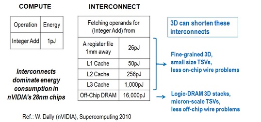
There are many applications that benefit from small TSV sizes. Fig. 1 describes the basic motivation - wires consume a lot more energy than transistor-based computation today, and 3D can reduce lengths of these wires. Micron-scale TSVs can reduce chip-to-chip wire lengths, but smaller TSVs are needed to reduce on-chip wire lengths.
- Short on-chip wires in logic cores and SoCs: Components within a single logic chip can be stacked atop each other to shorten on-chip wires. This leads to smaller gates, since these gates need to drive less wire capacitance. The result is reduced power and die size. Analyses show that a 2x reduction in power, a 2x reduction in silicon area and a 4x reduction in chip footprint may be possible by doubling the number of 3D stacked layers (link).
- Logic-SRAM stacking: The requirements of logic devices and SRAM on a chip are very different today. SRAM circuits typically require just 4 metal levels compared to 12 for logic circuits. SRAM transistors have different channel length, oxide thickness and threshold voltage compared to logic transistors too. In this scenario, it makes sense to stack SRAM and logic in 3D. The SRAM layer can be optimized for 4 metal levels and SRAM-type transistors, thereby saving cost.
- nMOS and pMOS stacking: Today's nMOS and pMOS transistors have different gate stacks, strain layers, implants and wells. Separate lithography steps are required for all of these. To save cost, one could stack the nMOS and pMOS atop each other. This reduces standard cell area too. Analysis from IBM shows that 30-40% reduction in standard cell area is possible for inverters, NAND and NOR cells by stacking nMOS and pMOS layers atop one another. Smaller standard cells result in shorter wires, improving power and performance.
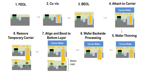
Like many engineers, I believe understanding a problem is important for figuring out a solution. So, let's analyze why today's TSVs are so fat. Fig. 2 shows a typical process for high-density 3D-ICs.
Step 5: Wafer thinning - Aspect ratio limitations of TSV manufacturing processes nowadays are around 10:1. To get 1um diameter TSVs, one needs to have a 10um thick silicon layer. For this scenario, during the thinning step, a 775um thick wafer needs to be thinned down to 10um +/- 1um (10% tolerance). This 1um tolerance is very hard to achieve at high throughput. Many manufacturers take the easy way out and thin the silicon wafer from 775um to 50um +/- 5um (10% tolerance). For an aspect ratio of 10:1, a 50um silicon thickness will lead to 5um diameter TSVs.
Step 7: Wafer alignment - In this step, the top and bottom layers are aligned with each other and bonded. Misalignment occurs due to several reasons:
- 3D align and bond tools on the market often do not have the stable alignment stages and image capture/storage required for sub-500nm pitch TSVs.
- Co-efficient of thermal expansion (CTE) mismatch between the top and bottom layers, wafer bow, thermal and stress induced flow of temporary bonding adhesives, localized bonding imperfections and other issues can cause um-scale misalignment.
In this section, I will summarize evolutionary ways to improve today's TSV technologies. IBM and MIT Lincoln Labs are the pioneers in this area, as are image sensor makers such as Sony and Omnivision.
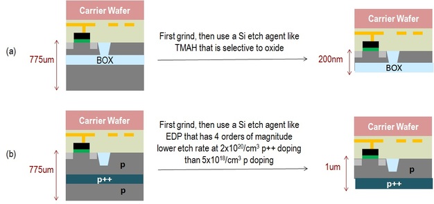
Wafer thinning techniques - Fig. 3 shows approaches to reduce wafer thickness from 775um to less than 1um. The method in Fig. 3(a) works for SOI wafers. Buried oxide layers of SOI wafers are used as etch stops to get low silicon thickness with sufficient precision. An alternative approach for bulk silicon wafers is shown in Fig. 3(b). Silicon etch solutions such as EDP have orders of magnitude lower etch rates for p++ silicon compared to p silicon. One could therefore use a p++ layer in a silicon wafer as an etch stop. Both these techniques are starting to be used in manufacture of back-side illuminated image sensors.
Techniques to improve alignment accuracy - For high density TSVs, companies prefer to use glass carrier wafers at present. The transparency of glass, combined with low silicon thickness of transferred films, allows one to look through the top wafer and align. Limitations of 3D alignment tools can be overcome with this technique. In addition, if glass carrier wafers are used, adhesives for attaching silicon to a carrier wafer can be optically debondable. Optically debondable adhesives are more stable at the high temperatures needed for bumpless bonding.
Besides using glass carriers, one could do a few more things:
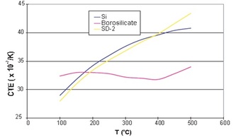
- Use CTE matched carrier wafers - Even if you use borosilicate glass with an excellent CTE match with Si, a small CTE mismatch is introduced at bond temperatures. For example, at 300C, silicon wafer diameter can increase by 314um while borosilicate glass diameter can increase by 264um. This difference in diameter can introduce alignment error. If you want to get sub-500nm pitch, costlier glasses that have CTE-match with silicon at various temperatures are required (Fig. 4(a)).
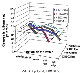
- Use oxide-to-oxide bonding - For fine-grain 3D, oxide-to-oxide bonding is the technique of choice due to the low temperatures involved vs. Cu-Cu bonding. Lower temperatures reduce CTE mismatch errors. In an oxide-to-oxide bonding process, a weak bond is formed at room temperature. Following this, a post-bond anneal (~300C) is done to get a stronger bond. The alignment got at room temperature is largely maintained. Less than 400nm misalignment is introduced by the post-bond anneal (Fig. 4(b)).
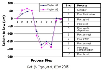
- Use wafer bow compensation - Wafers can frequently have bow of 50-100um, making sub-micron alignment accuracy difficult while bonding. IBM and MIT have developed wafer bow compensation schemes to reduce this. For example, one could deposit thin films on back sides of wafers to compensate partially for the wafer bow. See Fig. 4(c).
Figure 4(a)-(c) from left to right: (a) CTE match of various glasses with silicon. (b) Change of alignment after post-bond anneal. (c) Wafer bow compensation schemes.
IBM built prototypes utilizing many of these techniques. SOI wafers and buried oxide etch stop layers enabled transfer of thin silicon. CTE-matched borofloat glass carriers, oxide-to-oxide bonding and wafer bow compensation schemes were used. IBM's best prototypes had a TSV pitch of 6.7um, and they said 2um pitch would be possible when bonders with sub-0.5um alignment accuracy are available (which is the case today). Essentially, we can reduce TSV pitches from the 20um we get in the marketplace today to around 2um. I believe it may be possible to lower TSV pitches to less than 500nm by improving processes further. Please see slides of my talk for details.
The Monolithic 3D Path
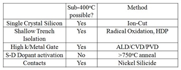
With monolithic 3D technology, additional transistor layers are constructed monolithically atop Cu/low k layers. This could lead to TSV size close to minimum feature size, which is needed for many of the fine-grain 3D applications described above. Fig. 5 indicates the main barrier to creating high-quality transistors at Cu/low k compatible temperatures (sub-400C) is dopant activation.
Fig. 6 describes one approach to overcome this problem, which utilizes recessed channel transistors. These have been used in DRAM manufacturing since the 90nm node, and are known to be competitive with standard planar transistors. As can be seen in Fig. 6, high temperature dopant activation steps are conducted before transferring bilayer n+/p silicon layers atop Cu/low k using ion-cut. For ion-cut, hydrogen is implanted into a wafer at a certain depth creating a defect plane. Following this, the wafer is bonded to the bottom device layer using oxide-to-oxide bonding. The bonded structure can now be cleaved at the hydrogen plane using a 400C anneal or a sideways mechanical force. CMP is done to planarize the transferred surface. Transferred layers are unpatterned, therefore no misalignment issues occur while bonding. Following bonding, sub-400C etch and deposition steps are used to define the recessed channel transistor. This is enabled by the unique structure of the device. These transistor definition steps can use alignment marks of the bottom Cu/low k stack since transferred silicon films are thin (usually sub-100nm) and transparent. Minimum feature size through-silicon connections can be produced due to the excellent alignment.
A few points about Fig. 6: (i) All materials, process steps and device structures are well-known and are used in high-volume manufacturing (ii) The original donor wafer with n+ and p layers can be reused after layer transfer. This is an advantage over today's TSV processes, where one spends time and cost etching away a 300mm wafer that costs $120. (iii) Though-silicon via connections are minimum feature size, enabling large improvements (As described previously, benefits can be 2x lower power, 2x lower silicon area by doubling the number of device layers. nMOS and pMOS stacking is possible.) The main risk is the use of DRAM-type recessed channel transistors in logic technologies. My somewhat biased view is that recessed channel transistors have been used in DRAM manufacturing since the 80nm node, so they may not be difficult for logic manufacturers to bring up and make competitive (especially for low-power applications).
Anyway, it is time to sign off now. If you are at the IEEE 3D System Integration Conference in Japan next week, don't forget to attend MonolithIC 3D Inc.'s presentation. I will be giving an invited talk titled "Monolithic 3D-ICs with Single Crystal Silicon Layers".
Disclosure: I work at MonolithIC 3D Inc., a company developing monolithic 3D technologies. I have tried to be as unbiased as possible while describing 3D-TSV and monolithic 3D technologies. However, if you disagree with something written in this blog post, please let me know in the comments section. I would welcome the discussion. Thank you.
- Post by Deepak Sekar



 RSS Feed