In today's blog post, we'll look at TSV sizes for TSMC, IBM and others, and discuss technical reasons for the fat TSVs we are seeing... I'll present solutions to this issue at the IEEE CPMT Society on Wednesday.
Many companies such as TSMC, IBM, ST Microelectronics and others have announced 3D Through-Silicon Via (TSV) technologies. In Figure 1, I've summarized key aspects of these technologies. You'll notice TSV sizes are in the micron range, while feature sizes are in the nm range.
In case you're wondering what I mean by keep-out zones in Figure 1: TSVs are typically constructed of copper, which has co-efficient of thermal expansion (CTE) 17ppm/K. This is very different from the CTE of silicon (2.3 ppm/K). Due to this, TSVs introduce stress on transistors placed close to them, impacting transistor performance. To avoid these issues, keep-out zones exist around TSVs. Transistors are not placed within these keep-out zones.
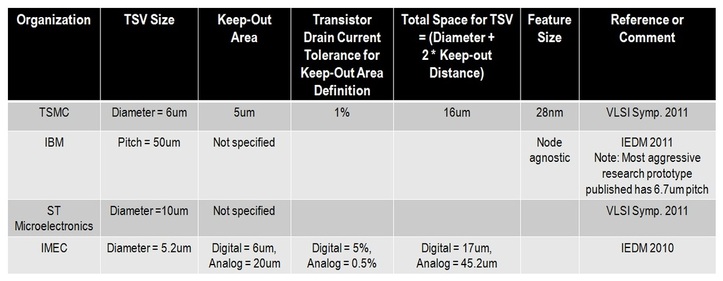
Figure 1: Parameters of TSV technologies from TSMC, IBM, ST Microelectronics, etc
TSV sizes are big today, but could things change in the future? Figure 2 shows projections from the International Technology Roadmap for Semiconductors. You'll notice that if we continue extending current technology, minimum TSV sizes will remain in the micron range for the foreseeable future...
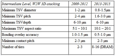
Figure 2: 3D-TSV technology roadmap from the 2010 International Technology Roadmap for Semiconductors.
Let's now try and understand why TSV sizes are so high. Figure 3 shows the process flow for a state-of-the-art 3D-TSV technology. The main steps that limit TSV sizes are:
- Wafer thinning - The best aspect ratio possible for TSV manufacturing is around 10:1 right now. So, if you have to make a 1um diameter TSV, you will need to thin a 775um thick wafer to 10um +/- 1um, which is immensely challenging, especially considering throughput requirements. Many companies therefore make their lives easier by thinning 775um wafers to 50um +/- 5um, which gives 5um diameter TSVs for 10:1 aspect ratio. Manufacturing throughput is also better in this case. Of course, this comes at the expense of TSV size.
- Alignment and bonding - During the "align and bond to bottom layer" step in Figure 3, several issues arise. Co-efficient of thermal expansion between layers being bonded is often different, causing misalignment when temperature changes during bonding. Processed wafers that are being bonded may have different bow, introducing more misalignment. The nature of the substrate (eg. transparent or opaque) can change alignment accuracy too. As mentioned in Figure 2, bonding overlay accuracy is around 1-1.5um for state-of-the-art technologies today.
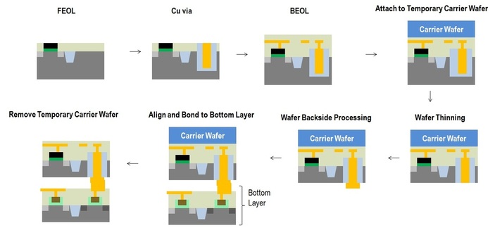
Figure 3: Process Flow for a State-of-the-Art 3D-TSV Technology (Not to Scale).
TSV sizes in the micron range are great for many applications, such as stacking DRAM with logic, wide I/O DRAM, back-side illuminated image sensors and heterogeneous chip stacking. But what if TSV sizes can be made smaller? It could open up a whole new set of applications... So, how can we make these fat TSVs slim down? (yes, near the New Year, slimming down is on everyone's mind!) What are the applications for small TSV sizes? If you'd like to know more, please attend my talk on Wednesday 11th January at the IEEE CPMT Society. Below are details of the talk... Don't forget to RSVP at www.cpmt.org/scv/meetings/cpmt1201.html
- Post by Deepak Sekar
- Post by Deepak Sekar


 RSS Feed