We’ve often heard about foundries struggling to ramp-up yield of High-k/Metal Gate technologies. In this blog post, I’ll talk about some of the key issues involved.
Last week, Gartner and KLA-Tencor talked about the yield issues surrounding High-k/Metal Gate (HKMG) technology in foundries. EETimes had a pretty widely circulated story on this phenomenon. This news matches what I’ve been hearing from friends in the industry – some foundries had single digit yield numbers with HKMG a few months back! Repeated delays with HKMG offerings have cost many top foundry executives their jobs too (see [1], [2], [3], [4]). Figure 1 might indeed be a realistic scenario...
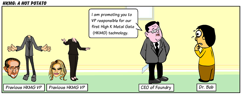
Figure 1: A situation in a hypothetical foundry.
All of us know strategic decisions made by management are a key determining factor behind success or failure of a technology. What strategy should Dr. Bob, the new HKMG VP for our hypothetical foundry in Figure 1, adopt? Let’s brainstorm about that:
Gate-First or Gate-Last?
There are two major approaches to HKMG implementation, gate-first or gate-last, depending on whether the gate is formed before or after high-temperature anneals required for the source-drain. Figure 2 shows process flows for these approaches. There are multiple trade-offs involved with this decision:
- Constrained layouts for Gate-Last: The Gate-Last process requires a Polish (CMP) step at the end. Due to this, layouts are constrained and layout density may be impacted versus a Gate-First process. Companies are being forced to use constrained layouts due to litho issues anyway, so many foundries such as TSMC don’t consider this a major issue.
- Improved strain: The gate-last process enhances strain effects on transistor performance quite significantly, leading to better performance. See this paper for more details.
- pMOS work-function: Due to its thermal profile, a gate-first process has several challenges with achieving the 5eV pMOS work-function required for high-performance (low Vt) applications. A gate-last process fares much better. More details can be found here.
- Thermal budget issues: During gate-first processing, temperatures in the 900C+ range are used, which are higher than the crystallization temperature for hafnium oxide. Crystallization can produce grain boundaries, which may potentially lead to variability, spatially varying electric fields (reduced mobility) and higher trap density. To avoid crystallization issues, many companies dope other materials such as Si into Hafnium oxide, which unfortunately lowers the effective k. High T can also lead to thicker interfacial oxide between the silicon and the high k dielectric. The number of gate electrode choices that can withstand high T is limited too, which makes finding a solution harder.
Based on these trade-offs, it certainly looks like Dr. Bob should go for Gate-Last. The risk is significantly lower – challenging issues with pMOS Vt and thermal budget are tackled.
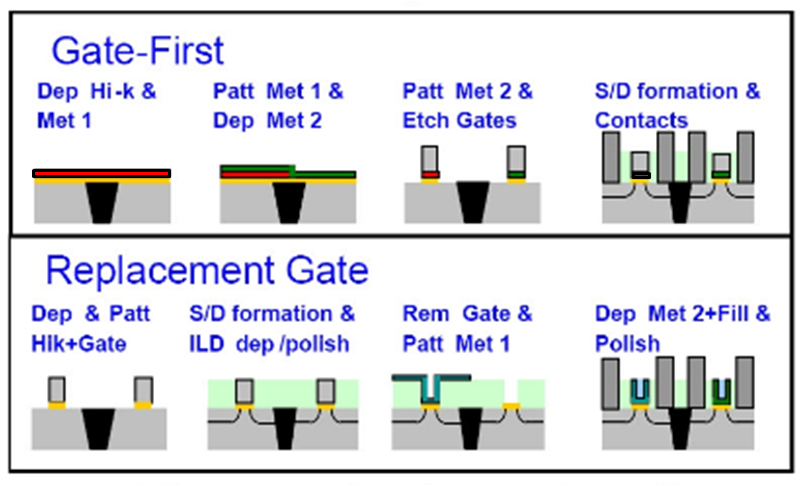
Figure 2: Gate-First and Gate-Last (also called Replacement Gate) Process Flows.
Deposition Method
Companies have experimented with MOCVD and ALD for high k dielectric deposition. It certainly looks like Dr. Bob should choose ALD... research indicates its film characteristics are better than MOCVD, and it offers better uniformity, surface roughness and thickness control. For ALD Hafnium Oxide deposition itself, two precursors are commonly used – TEMAHf (liquid source) and Hafnium Chloride (solid source). The Hafnium Chloride source has been found by several researchers to have positive attributes such as lower leakage, higher density and/or smoothness. So, Dr. Bob’s strategy should probably be – do ALD Hafnium Oxide with a Hafnium Chloride solid source.
Dope with Si or N?
Several gate dielectrics have been explored: Hafnium oxide, HfSiO and HfSiON. Each of these has its own tradeoffs. HfSiO has a lower k value than Hafnium oxide, but could provide higher crystallization temperature and higher mobility. Additional N incorporation into HfSiO could provide increased thermal stability and improve effective k value, but reduces mobility. To get the highest k film for a Gate-Last process, Dr. Bob should probably go with Hafnium oxide – interfacial silicon oxide and HfSiO form during the Hafnium Oxide deposition anyway, which helps with mobility issues.
Metal Gate Materials
Companies use TiN, TiAlN, TiSiN, TaN, TaAlN, TaSiN. Work functions of these materials can be tuned by changing the percentage of different elements in the compound and also by adding cap layers. Dr. Bob should play with these different materials smartly and tune work function based on his requirements.
One of the reasons why foundries have struggled with HKMG is because they’ve gone into research mode and tried to invent too many things. For example, if one starts evaluating 3 different gate dielectrics each in combination with 4 deposition recipes, 5 gate electrodes and 5 etch/clean recipes, that will lead to 3*4*5*5 = 300 different experiments and 1-2 years of work!! A good project manager would use his judgment, prior work and theoretical understanding to simplify the sample space and prevent his team from getting lost in wrong directions. With Dr. Bob focusing his team on gate-last, ALD deposition of Hafnium Oxide with Hafnium Chloride precursors and use of TiN/TiAlN metal gates, they can make it to manufacturing much faster, can’t they? I’d like to add that even after these strategies are selected, the HKMG problem is a hugely challenging one... Intel, which has successfully taken HKMG to production for two generations, calls it the biggest change to transistors since the 1970s!
The other issue to consider is how we are making dramatic changes to transistor architecture almost every generation. Even before we recovered from HKMG, many companies are taking the Finfet into production! How long will companies continue “band-aiding” 2D scaling? Will they go the monolithic 3D route instead? When you scale with monolithic 3D, you use the same feature size and transistors and just add additional device layers... your wires are shorter and you don’t need new litho tools or major transistor overhauls!
- Post by Deepak Sekar


 RSS Feed