We have a guest contribution today from Zvi Or-Bach, the President and CEO of MonolithIC 3D Inc. Zvi discusses Monolithic 3D's potential impact on the semiconductor industry...
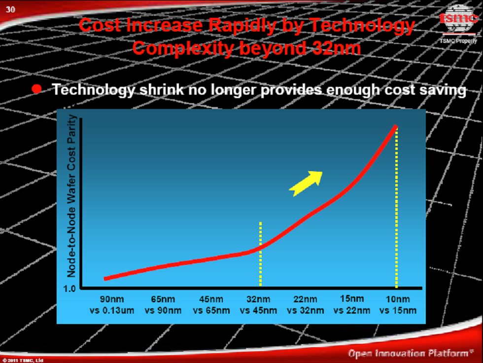
"The path is clear for continued semiconductor scaling using FinFETs for the next decade, down to the 7-nm node". Yet, at the time, EE Times quoted Chi-Ping Hsu, senior vice president at Cadence: “Process R&D, for instance, jumped from $1.2 billion at 32/28nm to between $2.1 billion and $3 billion at 22/20nm". So clearly the “clear path” is associated with escalating costs.
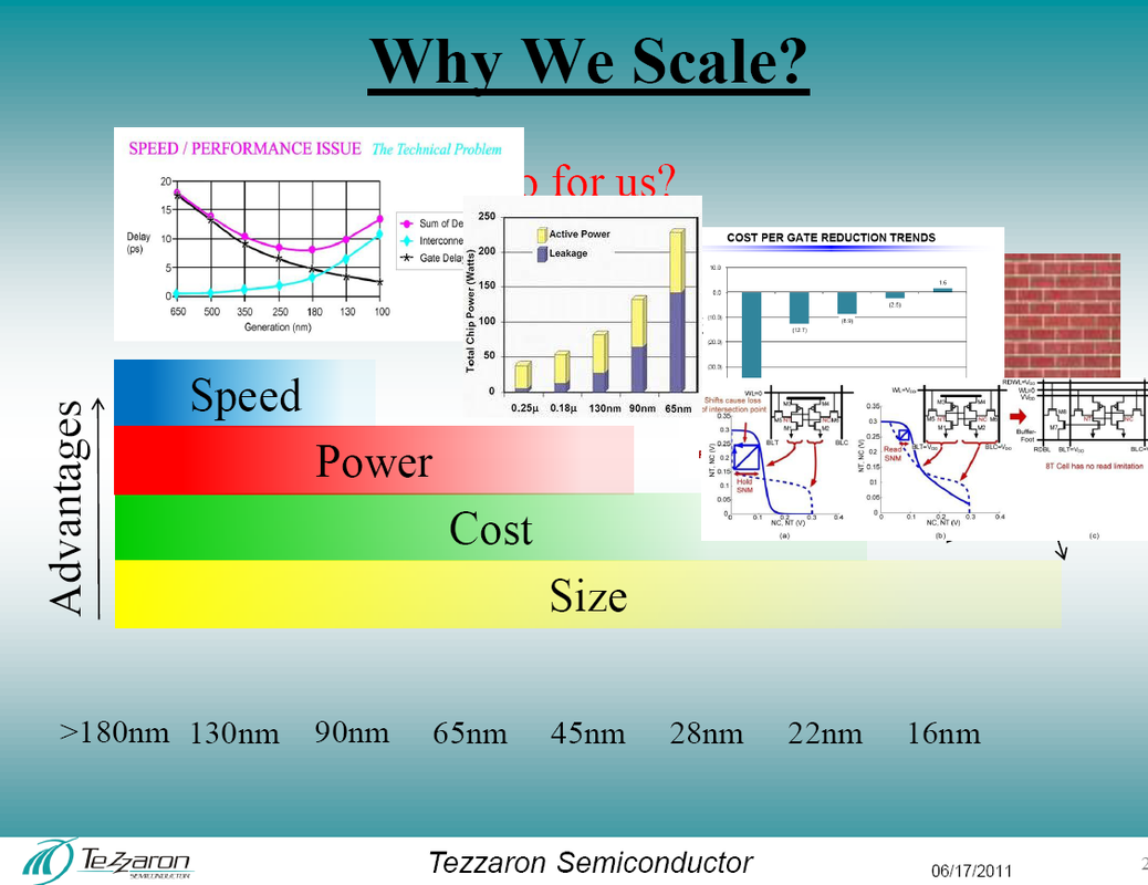
But the bigger question is: “What are we getting for the money?” After looking at the following chart from Bob Patti of Tezzaron you might want to argue “Not Much!”, as it shows the diminishing return in speed, power, and cost.
So, why is dimensional scaling still the prevailing direction and course of the industry?
From Wikipedia, the free encyclopedia – “A disruptive technology or disruptive innovation is an innovation that helps create a new market and value network, and eventually goes on to disrupt an existing market and value network (over a few years or decades), displacing an earlier technology there. The term is used in business and technology literature to describe innovations that improve a product or service in ways that the market does not expect, typically first by designing for a different set of consumers in the new market and later by lowering prices in the existing market.”
Clayton M. Christensen and others have shown numerous of cases where the leading vendors insisted on pursuing the same course by employing incremental innovation and ignoring the new technology that later turns out as a game changing innovation.
50 years of success with dimensional scaling has formed an extremely strong incremental innovation momentum and makes the decision to follow that course the most natural decision for the industry.
However, following the old course has been shown, time and time again, as a disastrous mistake when disruptive technology has emerged.
Now that monolithic 3D IC technology is shown to be possible and practical, it should be considered as the clear potential disruptive technology to be explored and studied.
Quoting Professor Fabian Pease of Stanford University: “Further feature size scaling will be difficult and will not provide as much benefit as before. Monolithic 3D IC techniques are required to keep Moore’s Law valid. Monolithic 3D is the future.”
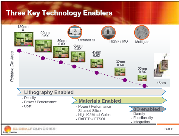
Or, as presented by Global Foundries, following chart:


 RSS Feed