Monolithic 3D Inc., the Next Generation 3D-IC Company
  • Home
  • Technology
    • Technology
    • Papers, Presentations and Patents
    • Overview >
      • Background
      • Why Monolithic 3D?
      • Paths to Monolithic 3D
      • Applications
    • Ion-Cut: The Building Block
    • Monolithic 3D Logic >
      • RCAT
      • HKMG
      • Laser Annealing
      • RCJLT
      • 3D Embedded RAM
      • 3D Gate Array
      • FPGA
      • Ultra Large Integration - Redundancy and Repair
    • Monolithic 3D Memory >
      • 3D DRAM
      • 3D Resistive Memories
      • 3D Flash
    • Monolithic 3D Electro-Optics >
      • 3D Image Sensors
      • 3D Micro-Displays
  • 3D-IC Edge
    • 3D-IC Edge
  • News & Events
    • News & Events
    • S3S15 Game Change 2.0 Video/P
    • Webcast
    • Webinar
    • Press Releases
    • In the News
    • Upcoming Events
  • About Us
    • About Us
    • History
    • Team
    • Careers
    • Contact Us
  • Blog
  • Simulators

"-Intel exec says fabless model 'collapsing"-'fab' or reality-?

5/5/2012

0 Comments

 
Picture
We have a guest contribution from Zvi Or-Bach, the President and CEO of MonolithIC 3D Inc. Zvi discusses about the latest news regarding the reversal of the trend from Foundry model back to the IDM model.

Are we facing a dramatic reversal of the trend from the Foundry model back to the IDM model???

Recently Rick Merritt of EE Times reported on his interview with Mark Bohr, "Mr. Process Technology at Intel," and wrote: "It’s the beginning of the end for the fabless model according to Mark Bohr."

Quite naturally this caused many responses, with the majority of them hinting that Intel is trying to break into the smart mobile space by sowing doubt in the future of the existing ecosystem around TSMC-ARM and multiple fabless vendors.

We recently wrote two very relevant blog entries:

Is NVIDIA in a Panic? If so, what about AMD? Other fabless companies? 04/02/2012
and
Why Samsung will give Morris Chang sleepless nights 02/05/2012


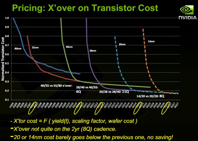
With recent reports about Qualcomm having issues with TSMC, Apple not being able to shift out from Samsung (their competitor) to TSMC, AMD having severe issues and trying to shift some of manufacturing from GlobalFoundries to TSMC, and straight out statements such as:  "NVIDIA deeply unhappy with TSMC, claims 20nm essentially worthless," one can't avoid the question: Are we facing a dramatic reversal of the trend from the Foundry model back to the IDM model???


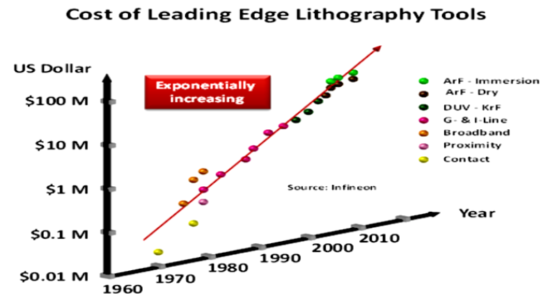
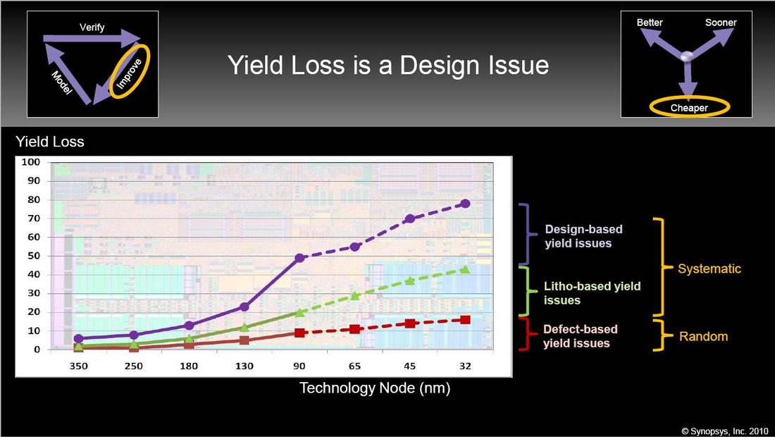
It does seem that advanced scaling these days provides a significant advantage to the integrated model, where trade-offs between design, library EDA, and manufacturing, provide a better end product. Such an integration advantage manifests itself with respect to yield, now that the majority of the yield losses are design-related rather than random defects, and to manufacturing cost, as some of the layers needs double or even triple/quad patterning. 


Accordingly, this might explain why both TSMC and GlobalFoundries recently announced investment in 3D IC processing lines (TSMC plans 3-D IC assembly launch early in 2013, GlobalFoundries installs gear for 20-nm TSVs). As the current scaling trend works against them, they both chose to move the game to a court where an ecosystem would be more powerful than corporate vertical integration.


We at MonolithIC 3D Inc. are very pleased to see 3D ICs becoming a key business strategy, and truly believe that adding monolithic 3D manufacturing capabilities will extend foundries’ strategic benefits even further. Monolithic 3D, with its 10,000x better vertical connectivity, provides an exciting alternative to pure dimensional scaling. Moore's law is about doubling the number of transistors, which could be easily achieved using existing process and lithography by simply doubling the number of layers carrying transistors. Scaling through the third dimension provides power, speed, and cost benefits similar – or even better -- than we once used to get from dimensional scaling (see "Why Monolithic 3D" for more information).


In addition, monolithic 3D provides benefits that cannot be achieved with dimensional scaling such as pulling out embedded memory into another layer on top of the logic. In a typical SoC the embedded memory may represent 50% of the die area and include hundreds of memory macros, requiring too many vertical connections for TSV but is a very simple task for monolithic 3D integration. A dedicated memory layer also allows optimizing the first layer for logic and the second layer for memory, which could be even a DRAM rather than SRAM, and would need fewer costly metal layers. Another advantage is the realization of logic-cone-level logic redundancy, as described in Monolithic 3D IC Could Increase Circuit Integration by 1,000x and in Redundancy & Repair with Monolithic 3D.


In summary, the current trend in the semiconductor industry indicates that IDMs have a significant advantage in the leading edge dimensional scaling race. Foundries recognize it and are responding by adding 3D capabilities. They could do even better by also adding monolithic 3D. 
submit to reddit
0 Comments

Is NVIDIA in a Panic? If so, what about AMD? Other fabless companies?

4/2/2012

4 Comments

 
Picture
We have a guest contribution from Zvi Or-Bach, the President and CEO of MonolithIC 3D Inc. Zvi discusses NVIDIA's presentation at the International Trade Partner Conference (ITPC) forum last November.

Recently I read a very uncommon report title: "NVIDIA deeply unhappy with TSMC, claims 20nm essentially worthless". Quoting directly: “One of the unspoken rules of customer-foundry relations is that you virtually never see the former speak poorly of the latter. Only when things have seriously hit the fan do partners like AMD or NVIDIA admit to manufacturing problems... That’s why we were surprised - and our source testified to being stunned - that Nvidia gave the following presentation at the International Trade Partner Conference (ITPC) forum last November”
Picture
Figure 1
The only explanation I can come up with is that NVIDIA is in a panic. And according to Andy Grove’s “Only the Paranoid Survive” I believe NVIDIA will overcome the challenge, and at the later part of this blog we will present our view for an action plan. But first let’s try to understand what the issue is about.

It all starts with the diminishing return of dimensional scaling. This time it is about costs. Dimensional scaling requires continual improvements in lithography capability, and is primarily driven by the rapidly escalating cost of lithography, as illustrated by the following chart:
Picture
Figure 2
Now that the cost of lithography dominates the cost of Fabs and accordingly the cost of a finished wafer, the cost reduction associated with getting more dies per wafer (scaling) becomes neutralized by the higher cost of wafers. This was recently articulated in View Point in EE Times by Dr. Handel Jones and illustrated by the following chart.
Picture
Figure 3
Furthermore, pure foundry leader TSMC publicly showed the issue as seen in the following chart
Picture
Figure 4
And accordingly the following charts from NVIDIA present the same trend in a very clear way:
Picture
Figure 5
Moreover, another chart by NVIDIA shows the higher cost of wafers eating away at the benefits of dimensional scaling:
Picture
Figure 6
But this is clearly not TSMC’s fault. So why: "NVIDIA deeply unhappy with TSMC, claims 20nm essentially worthless"? And why would NVIDIA care? If the price will stop going down they should be happy to be able to charge more as long as their competitors need to do the same. And it is hard to believe AMD would see different curves from TSMC??

But careful review of the bullet slide above and the bullet slide below might reveal NVIDIA’s underlying  concerns.
Picture
Figure 7
Both slides indicate real concerns and reflect some form of panic.

It seems to me that the key words are “Virtual IDM”, which are the only highlighted words of the second bullet slide but do appear also in the first one.
“When business ($) gets in the way, apply “First principle”, the principle of one company, one virtual IDM company”. I was not aware of this “First principle”. I thought our first principle is open competition, and individual companies are supposed to work as such and not as one company I believe we have some laws - Antitrust - against acting as one company instead of individual company.
Yet, NVIDIA does have one strong IDM competitor - Intel. Could it be that Intel’s costs are different??

I don't know but it does remind me of a previous blog I wrote: Required Change in EDA Vendors’ Role and Reward vs. Scaling Yield. In that blog we tried to understand the implication of dimensional scaling on yield, and more specifically on the systematic yield losses which are design related. The following chart was presented then
Picture
Figure 8
In that blog we suggested that an IDM would have a significant advantage over the “partnership” of Fabless-Fab-EDA.

Looking again on the cost related chart one can clearly see NVIDIA pointing to the importance of yield. But I believe they should not blame just TSMC as it would seem to me that the EDA part is just as important.
NVIDIA, TSMC and the other fabless companies and partners (EDA, etc.) should strategically consider the issues associated with dimension scaling, which seem to strongly benefit the IDMs. Such strategic evaluation should include a serious look into the better alternative to dimensional scaling - the monolithic 3D, or as we call it, scaling Up!!!
submit to reddit
4 Comments

"Chip 2020" - The End of Scaling is 2020 - or not - Book Review

3/5/2012

0 Comments

 
Picture
We have a guest contribution from Zvi Or-Bach, the President and CEO of MonolithIC 3D Inc. Zvi discusses about "Chip 2020" book review. 

A recent book review by Peter Clarke on this wonderful new book by Bernd Hoefflinger caught my eye, and also reminded me of an old connection I have with Hoefflinger.

Early in the 90's I had the pleasure to collaborate with Hoefflinger, who at that time was the director of the Institute for Microelectronics Stuttgart (IMS CHIPS). I was the CEO of Chip Express then and we worked together to demonstrate that applying Direct-Write-eBeam to a Chip Express wafer could lead to a very effective Gate-Array prototyping scheme and to low volume production of those Gate-Arrays.

It was great pleasure to reconnect and to read "Chip 2020"
I highly recommend this book as it provides an update view of the Semiconductor Industry by a group of known experts in our field.
The book provides a concise review how we got here and what is ahead for us up to the year 2020.

The book presents a now more common view that the scaling that got us here is gone, and that there are concrete red-bricks for dimensional scaling beyond 2020. Primarily:

1. As gate sizes reach ~10nm we would have nominally 6 atoms of impurity in the channel with a commensurate variation that would constrain effective use of the transistor -see Fig. 1.1

Picture
2. As lithography tools are already forced to use double exposure/processing it has became unclear if an effective lithography is going to be available to move forward. See the Table 8.3 below, provided by Burn J. Lin of TSMC
Picture
Clearly the future cost of lithography eats away at the cost advantage of dimensional scaling.

Hoefflinger presents some options to tackle these challenges as detailed through the book and with respect to specific segments of the industry. The following Fig. 3.1 presents these future technologies:

Picture
At MonolithIC 3D we were pleased to see the important role given to 3D IC in the book as shown in the Fig. 3.1 above.

In short I fully agree with Peter Clarke’s statement: "The book offers some far-reaching and fundamental insights" and I highly recommend the book to semiconductor technologists who are looking forward toward the next decade of progress in the field.


submit to reddit
0 Comments

Monolithic 3D IC Could Increase Circuit Integration by 1,000x

12/15/2011

1 Comment

 
Picture

We have a guest contribution from Zvi Or-Bach, the President and CEO of MonolithIC 3D Inc. Zvi introduces a very interesting idea that could have huge implications for high-performance computing.


Read More
1 Comment

"Achieving Success In The Age of Nano Tech"

10/20/2011

0 Comments

 
Picture
We have a guest contribution today from Zvi Or-Bach, the President and CEO of MonolithIC 3D Inc. In this post, Zvi shares his perspective on where the industry is going after attending the recent Future Horizons conference (IEF-2011).


Read More
0 Comments

The Boiling Frog Syndrome and the Semiconductors Industry

9/15/2011

0 Comments

 
Picture

We have a guest contribution today from Zvi Or-Bach, the President and CEO of MonolithIC 3D Inc. In this post, Zvi shares his perspective on where the industry is going.


Read More
0 Comments

Embracing Talent as a Path for Long Term Sustained Recovery of US Economy

8/11/2011

1 Comment

 
Picture

We have a guest contribution today from Zvi Or-Bach, President and CEO of MonolithIC 3D Inc. In this blog-post, Zvi discusses a topic he is passionate about: immigration policy for the United States.


Read More
1 Comment

MonolithIC 3D is a Finalist of the “Best of Semicon West”!

7/7/2011

1 Comment

 
Picture

We have a guest contribution today from Zvi Or-Bach, MonolithIC 3D Inc.'s President and CEO. Zvi talks about some good news we received from the Semicon West committee recently.


Read More
1 Comment

Guest Contribution: Invited Talk at the 3D satellite workshop at the TIPP2011

6/16/2011

0 Comments

 
Picture
This week has been a busy week for our company. We were invited to speak at three different forums across the continent! Zvi Or-Bach, our President and CEO, went to Chicago to speak at a 3D workshop at the TIPP 2011. I went to speak at a 3D workshop at San Jose and Brian Cronquist, our VP of Technology, went to Canada to speak at the CMOS Emerging Technologies workshop. In this blog-post, Zvi discusses his time at the 3D workshop @ Chicago.


Read More
0 Comments

Guest Contribution: Embedded Memory and Monolithic 3D

6/2/2011

0 Comments

 
Picture

We have a guest contribution today from Zvi Or-Bach, the President and CEO of MonolithIC 3D Inc. In this post, Zvi discusses the implications of monolithic 3D for embedded memories.


Read More
0 Comments
<<Previous

    Search Blog


    Meet the Bloggers


    Follow us


    To get email updates subscribe here:


    Recommended Links

    3D IC Community
    3D IC LinkedIn Discussion Group

    Recommended Blogs

    • 3D InCites by Francoise von Trapp
    • EDA360 Insider by Steve Leibson
    • Insights From the Leading Edge by Phil Garrou
    • SemiWiki by Daniel Nenni, Paul Mc Lellan, et al.

    Archives

    May 2023
    March 2022
    December 2021
    August 2021
    August 2018
    July 2018
    May 2018
    October 2017
    September 2017
    December 2016
    September 2016
    August 2016
    November 2015
    October 2015
    September 2015
    July 2015
    June 2015
    May 2015
    April 2015
    March 2015
    February 2015
    October 2014
    September 2014
    August 2014
    July 2014
    June 2014
    May 2014
    April 2014
    March 2014
    February 2014
    January 2014
    December 2013
    November 2013
    October 2013
    September 2013
    August 2013
    July 2013
    March 2013
    February 2013
    January 2013
    December 2012
    November 2012
    October 2012
    August 2012
    June 2012
    May 2012
    April 2012
    March 2012
    February 2012
    January 2012
    December 2011
    November 2011
    October 2011
    September 2011
    August 2011
    July 2011
    June 2011
    May 2011
    April 2011
    March 2011

    Categories

    All
    3d Design And Cad
    3dic
    3d Ic
    3d Nand
    3d Stacking
    3d Technology
    Brian Cronquist
    Dean Stevens
    Deepak Sekar
    Dram
    Education
    Heat Removal And Power Delivery
    Industry News
    Israel Beinglass
    Iulia Morariu
    Iulia Tomut
    Monolithic3d
    Monolithic 3d
    MonolithIC 3D Inc.
    Monolithic 3d Inc.
    Monolithic 3d Technology
    Moore Law
    Outsourcing
    Paul Lim
    Repair
    Sandisk
    Semiconductor
    Semiconductor Business
    Tsv
    Zeev Wurman
    Zvi Or Bach
    Zvi Or-Bach

    RSS Feed

© Copyright MonolithIC 3D Inc. , the Next-Generation 3D-IC Company, 2012 - All Rights Reserved, Patents Pending