Yes, we have made a commitment to make the semiconductor industry aware that Monolithic 3D is now possible and practical. So, when Grzegorz Deptuch, the chair for the 3D satellite workshop at the TIPP2011 conference, invited us to present, we were happy to accept.
Along came Tuesday, the day of the talk, and I had to wake up at 3 AM so I get to Chicago by afternoon and get back home after midnight - a really long day, but that is part of start-up life (Yes, I been living this life since 1984)
The first half of the workshop was all about TSV and various efforts towards implementing it in the US, Europe and Japan. Nothing new to report other than the fact that there are massive efforts all around the world, which is a clear indication that we are going to 3D-ICs.
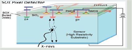
The second half got more interesting for me, with Yasuo Arai-san presenting SOI technology for monolithic and 3D integrated detectors http://3dic.fnal.gov/DetectorSOI.pdf. It felt like a good warm-up to our story. Arai-san reported on his company’s technology and around-the-world Multi-Project Wafer service that offers monolithic 3D sensors with two layers of SOI. The first layer is the bulk silicon carrying the sensors, while the thin layer on top of the oxide carries the sensor electronics.
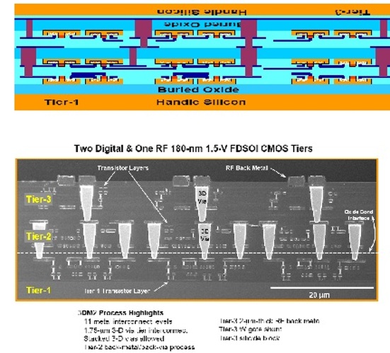
The following presentation from MIT Lincoln Labs (MIT-LL) warmed-up the audience even more for our talk. As many of you know, MIT-LL has been driving 3D integration for years. The MIT-LL technology is about as they call it - Through Oxide Via (TOV) - integrating layers of 6um vs. the 50um of the conventional TSV.
The latest update from MIT-LL on their technology:
The approach is to leverage the oxide of the SOI wafer as an etch stop. So using a carrier the MIT-LL process takes a processed wafer, flips it on top of another processed wafer, and uses their specially-made aligner to bond these two wafers face-to-face at high precision (~0.3um). Then, they etch the upper wafer all the way to 'SOI' oxide effectively trimming the upper layer to ~ 6um. Following this, they open the Through-Oxide Via and process the via and additional interconnections. Interestingly, MIT-LL has just upgraded to 8" operation and offer a Multi-Project Wafer (MPW) service.
Bob Patti, the CTO of Tezzaron, gave the next talk which provided even more background to our presentation. It was most reinforcing to have Bob articulating why scaling-down has reached the point of diminished to no-return, and the industry path forward should be 3D integration. "In 2004 Tezzaron demonstrated the world's first successful wafer-stacked 3D-ICs with TSV, including microprocessors, sensors, and SRAM devices", according to their website <http://www.tezzaron.com>. Tezzaron offers a via-middle process providing an aggressive TSV diameter of about 1m. They collaborate with Globalfoundries and even offer MPW through MOSIS <http://www.mosis.com/tezzaron/>. Bob presented multiple actual 3D cases where 5x performance improvement and 10x power reduction were achieved vs. 2D. An important success factor has been optimizing the architecture leveraging the 3D attribute for achieving these benefits. It seems that Tezzaron is now betting on their 3D DRAM design which offers SRAM-type access times.
The audience was now “warmed-up” to the topic of my presentation, since they had started to hear some of the benefits of smaller-size through-silicon connections. I then stepped up to the podium to present our monolithic 3D technology, which offers 2500x to 10,000x the density of today’s TSV technology. I believe our company’s technology is a breakthrough that can give our industry two more decades of “Moore-type” progress.
Interestingly, as you could see from this blog-piece, the conference organizers had arranged the presentations in the increasing order of through-silicon connection density! It really felt as though MonolithIC 3D technology is the natural progression from prior work with the capacity to extend the 3D-IC’s benefits to a very wide range of applications. And while I am not sure scaling down has reached the point of no-return, it seems clear that the cost of scaling down has reached the point of 'no-can-do'. Adding the monolithic 3D technology would help extend the effective life of the processing equipment for much more than a single node which could be the key to make semiconductor progress financially viable.


 RSS Feed