
We have a guest contribution from Zvi Or-Bach, the President and CEO of MonolithIC 3D Inc. Zvi introduces a very interesting idea that could have huge implications for high-performance computing.
Since the invention of the Integrated Circuit by Jack Kilby and Bob Noyce, we been pursuing Moore's Law by doubling device integration every two years. Higher integration has been the key ingredient to end product cost reduction and performance improvement. It has been well documented and demonstrated in the literature that integrating functions that were spread on a PC board onto a single chip could provide order of magnitude reduction of operating power and similar benefits to cost and performance.
The following information was presented recently by Chris Malachowsky, nVidia's Founder and senior VP of research: [Reference]
The following information was presented recently by Chris Malachowsky, nVidia's Founder and senior VP of research: [Reference]
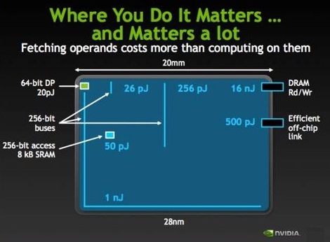
Figure 1: Energy estimates for different operations in nVIDIA's 28nm chips.
Simply stated: "loading the data from off chips takes >> 100x the energy" And clearly energy is today the limiting factor of future electronic systems and computing.
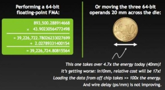
Figure 2: More estimates from nVIDIA.
So why are we not integrating more ?
The main limit to integration is yield. A secondary limitation is reticle size (~20x30 sq. mm). The semiconductor industry has an amazing skill to continuously improve device yield with scaling. At every new process node, yield gets improved so the new node with double the complexity gets yield similar to the previous node for about the same die size.
It is expected that a die of 10x10 sq. mm will have better than 50% yield. But as yield get reduced exponentially with die size, only in extreme cases, we see designs that are full reticle size and those tend to have very low yield.
MonolithIC 3D Inc. has innovated practical technologies to process multiple tiers of circuits with vertical connectivity comparable with horizontal connectivity. The technology utilizes very thin layers (<100nm) of mono-crystalline silicon, so each tier with its interconnect layers would add about 1 micron to the chip, allowing super high integration if the yield limit could be overcome.
Overcoming yield of non-repeating circuits (such as memory) is considered a hard problem. Trilogy System had attempted to do so with systematic application of "Triple Modular Redundancy" . Every logic gate and every flip-flop were triplicated with binary two-out-of-three voting at each flip-flop. Trilogy systems was known as one of the largest financial failures in Silicon Valley before the burst of internet/dotcom bubble in 2001. Aparently Trilogy's failure had a lasting effect and it seems that for over two decades no other attempts towards Wafer Scale Integration were made.
We believe that a new approach and new technology, alligned with many times larger market and far higher value for integration merits the development of super scale integration. The follwing provides an illustration of MonolithIC 3D Inc.'s 3D super scale integration scheme:
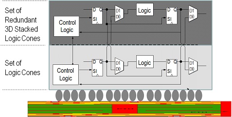
Figure 3: MonolithIC 3D Inc.'s super-scale integration scheme.
There are three primary ideas:
- Swap at logic cone granularity.
- Redundant logic cone/block directly above, so no performance penalty.
- Negligible design effort, since redundant layer is exact copy.
The first is the Scan Chain technology that enables circuit test where faults are identified at the logic cone level. The second is the 3D IC which enable replacement of defective logic cone by the same logic cone ~1 micron above.
Accordingly, by just building the same circuit twice one on top of the other with minimal overhead, every fault could be repaired by the replacement logic cone above. Such repair should have negligible power penalty and minimal cost penalty whenever the base circuit yield is about 50%. There should be almost no extra design cost and many additional benefits can be obtained (which we will discuss later)
So the immediate question would be how far can we go with such an approach ?
A simple back-of-the-envelope calculation should start with the number of Flip-Flops in a modern design. In today's designs we would expect more than 1 million F/F (logic cones). So, if we expect one defect, then the device with redundency layer would work unless the same cone is faulty on both layers which probability wise would be one in a million !
Clearly we have removed yield as a constraint to super-scale integration. We could even integrate 1,000 such devices!!!


 RSS Feed