
We have a guest contribution from Zvi Or-Bach, the President and CEO of MonolithIC 3D Inc. Zvi discusses NVIDIA's presentation at the International Trade Partner Conference (ITPC) forum last November.
Recently I read a very uncommon report title: "NVIDIA deeply unhappy with TSMC, claims 20nm essentially worthless". Quoting directly: “One of the unspoken rules of customer-foundry relations is that you virtually never see the former speak poorly of the latter. Only when things have seriously hit the fan do partners like AMD or NVIDIA admit to manufacturing problems... That’s why we were surprised - and our source testified to being stunned - that Nvidia gave the following presentation at the International Trade Partner Conference (ITPC) forum last Novemberâ€
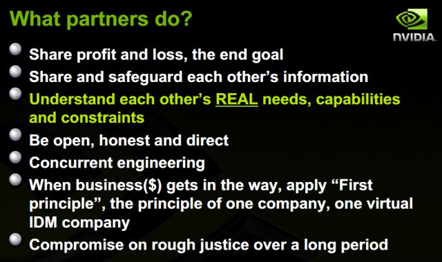
Figure 1
The only explanation I can come up with is that NVIDIA is in a panic. And according to Andy Grove’s “Only the Paranoid Survive†I believe NVIDIA will overcome the challenge, and at the later part of this blog we will present our view for an action plan. But first let’s try to understand what the issue is about.
It all starts with the diminishing return of dimensional scaling. This time it is about costs. Dimensional scaling requires continual improvements in lithography capability, and is primarily driven by the rapidly escalating cost of lithography, as illustrated by the following chart:
It all starts with the diminishing return of dimensional scaling. This time it is about costs. Dimensional scaling requires continual improvements in lithography capability, and is primarily driven by the rapidly escalating cost of lithography, as illustrated by the following chart:
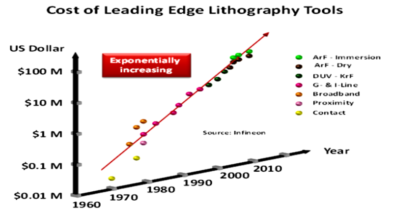
Figure 2
Now that the cost of lithography dominates the cost of Fabs and accordingly the cost of a finished wafer, the cost reduction associated with getting more dies per wafer (scaling) becomes neutralized by the higher cost of wafers. This was recently articulated in View Point in EE Times by Dr. Handel Jones and illustrated by the following chart.
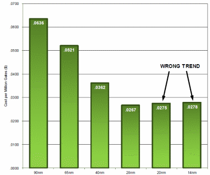
Figure 3
Furthermore, pure foundry leader TSMC publicly showed the issue as seen in the following chart
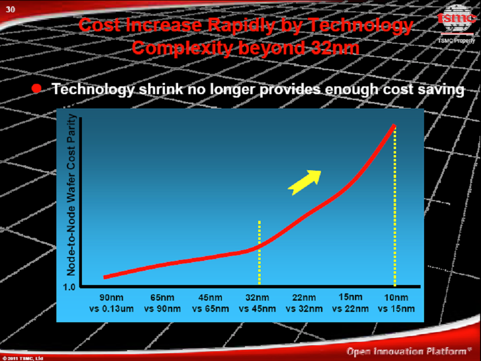
Figure 4
And accordingly the following charts from NVIDIA present the same trend in a very clear way:
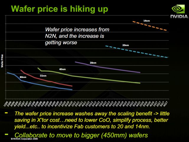
Figure 5
Moreover, another chart by NVIDIA shows the higher cost of wafers eating away at the benefits of dimensional scaling:
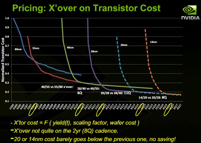
Figure 6
But this is clearly not TSMC’s fault. So why: "NVIDIA deeply unhappy with TSMC, claims 20nm essentially worthless"? And why would NVIDIA care? If the price will stop going down they should be happy to be able to charge more as long as their competitors need to do the same. And it is hard to believe AMD would see different curves from TSMC??
But careful review of the bullet slide above and the bullet slide below might reveal NVIDIA’s underlying concerns.
But careful review of the bullet slide above and the bullet slide below might reveal NVIDIA’s underlying concerns.
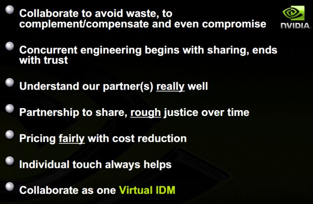
Figure 7
Both slides indicate real concerns and reflect some form of panic.
It seems to me that the key words are “Virtual IDMâ€, which are the only highlighted words of the second bullet slide but do appear also in the first one.
“When business ($) gets in the way, apply “First principleâ€, the principle of one company, one virtual IDM companyâ€. I was not aware of this “First principleâ€. I thought our first principle is open competition, and individual companies are supposed to work as such and not as one company I believe we have some laws - Antitrust - against acting as one company instead of individual company.
Yet, NVIDIA does have one strong IDM competitor - Intel. Could it be that Intel’s costs are different??
I don't know but it does remind me of a previous blog I wrote: Required Change in EDA Vendors’ Role and Reward vs. Scaling Yield. In that blog we tried to understand the implication of dimensional scaling on yield, and more specifically on the systematic yield losses which are design related. The following chart was presented then
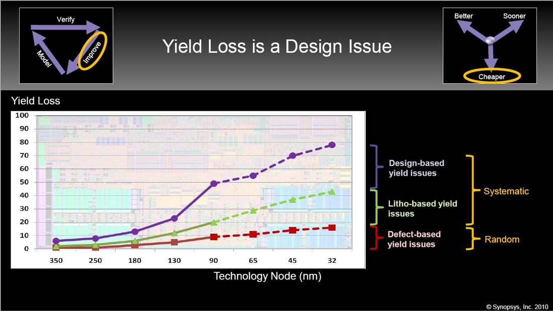
Figure 8
In that blog we suggested that an IDM would have a significant advantage over the “partnership†of Fabless-Fab-EDA.
Looking again on the cost related chart one can clearly see NVIDIA pointing to the importance of yield. But I believe they should not blame just TSMC as it would seem to me that the EDA part is just as important.
NVIDIA, TSMC and the other fabless companies and partners (EDA, etc.) should strategically consider the issues associated with dimension scaling, which seem to strongly benefit the IDMs. Such strategic evaluation should include a serious look into the better alternative to dimensional scaling - the monolithic 3D, or as we call it, scaling Up!!!


 RSS Feed