Will Intel 14 nm Continue the Historical Cost Reduction Curve
The above EE Times article provides the following numbers released by Intel on August 11:
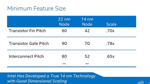
"Compared to Intel's 22nm process, it will have:
- 42nm fin pitch, down .70x
- 70nm gate pitch, down .78x
- 52nm interconnect pitch down .65x
- 42nm high fins, up from 34nm
- a 0.0588 micron2 SRAM cell, down .54x
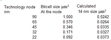
Let’s review the SRAM cell size of 0.0588µm². Yes, it is the smallest published size for a SRAM bitcell we have seen so far. Yet in our blog Intel vs. TSMC: An Update we wrote: "Accordingly, the 14nm node 6T SRAM size for conventional dimensional scaling should be 0.092 * (14/22)² =0.037 sq. micron. And if Intel can really scale more aggressively to compensate for the extra capital costs then their 6T SRAM at 14nm, it should be about 0.03 sq. micron or even smaller."
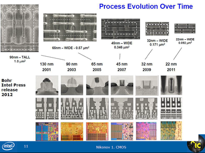
From Intel’s 2012 information release:
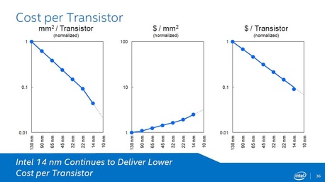
The recent Intel presentation argues for the continuation of historical scaling cost reduction to the 14 nm node as illustrated in the following Intel slide:
But the following Intel chart does not show a better than 2X density increase from 22nm to 14nm:
As well, this is before accounting for the increase in RC associated with the narrower metal lines. This would require insertion of many more buffers and repeaters, further reducing the effective density increase.
Furthermore, back to the SRAM bitcell. The announced size for the Intel 14nm bitcell as presented above is not going to help offset the increase in wafer cost.
So it seems this would be a subject matter for more comments and blogs. However, I see no reasons to change my prior statements published in the EE Time blog titled: 28nm – The Last Node of Moore's Law.


 RSS Feed