
We have a guest contribution today from Brian Cronquist, MonolithIC 3D Inc.'s VP of Technology & IP. Brian discusses about monolithic 3d technology for future scaling.
At the CEA-Leti Day July 8 during Semicon West, Hughes Metras, Leti's vice president of strategic partnerships for North America, introduced the lead talk about monolithic 3D technology as the "solution for scaling." The Leti device technology roadmap that Hughes presented showed monolithic 3D (M3D) as an alternative to scaling from the 2Xnm nodes to past 5 nm.Olivier Faynot, Leti's device department director and a well-known device scientist (with more than 170 papers/publications), entitled his talk "M3D, a disruptive approach for further scaling" and started with why the industry needs such a solution.
The majority of people in the industry agree that scaling past the 22nm node, though still quite technically feasible, has priced itself out of most markets. Faynot discussed the "what" (transistor costs are no longer decreasing) and the "why" (litho cost escalation and connectivity inefficiencies of energy and delay). Then he said, "If we just keep the current [2Xnm] technology, we can go farther in cost scaling."
Tech Design Forum's summary of a Qualcomm executive's DAC 2014 keynote offers more information on this crucial topic. So do a pair of EE Times blogs by Zvi Or-Bach.
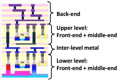
The solution is to build the stack sequentially in a monolithic fashion. (See Monolithic 3D IC Technologies.) Faynot described a process flow wherein the lower level (first layer) of transistors and its interconnect are made conventionally, some interlevel metal is crafted to help the vertical interconnection, and a second layer of monocrystalline silicon is layer transferred and oxide-oxide bonded at low temperature to the top of the interlevel metal dielectric. This is a blanket layer, so there are no alignment issues such as those suffered by the thick layer and pre-made (TSV) parallel processing flows. The layer that is transferred in M3D is very thin, so that direct alignment to the lower-level alignment marks can be made with conventional equipment, and conventional alignment tolerances (single-digit nanometers) can be achieved.
Upper-level transistors are formed utilizing solid-phase epitaxial regrow (SPER) for junction doping at 475-600°C and lower-temperature processing (less than 400°C) for things like gate stacks. The upper-level and inter-level vertical interconnect is then processed, again with full alignment capability to the lower layer. (Note that the lower-level transistor salicides are stabilized with platinum and fluorine/tungsten implantation to enable their survival at the 475-600°C SPER thermal exposure.)
In the Q&A session, Faynot was asked what the observed performance differences were between the upper-level and lower-level transistors. "Currently, we are achieving 95%" of the lower for the upper, he said. "We believe we can make 100%."
The majority of people in the industry agree that scaling past the 22nm node, though still quite technically feasible, has priced itself out of most markets. Faynot discussed the "what" (transistor costs are no longer decreasing) and the "why" (litho cost escalation and connectivity inefficiencies of energy and delay). Then he said, "If we just keep the current [2Xnm] technology, we can go farther in cost scaling."
Tech Design Forum's summary of a Qualcomm executive's DAC 2014 keynote offers more information on this crucial topic. So do a pair of EE Times blogs by Zvi Or-Bach.
The solution is to build the stack sequentially in a monolithic fashion. (See Monolithic 3D IC Technologies.) Faynot described a process flow wherein the lower level (first layer) of transistors and its interconnect are made conventionally, some interlevel metal is crafted to help the vertical interconnection, and a second layer of monocrystalline silicon is layer transferred and oxide-oxide bonded at low temperature to the top of the interlevel metal dielectric. This is a blanket layer, so there are no alignment issues such as those suffered by the thick layer and pre-made (TSV) parallel processing flows. The layer that is transferred in M3D is very thin, so that direct alignment to the lower-level alignment marks can be made with conventional equipment, and conventional alignment tolerances (single-digit nanometers) can be achieved.
Upper-level transistors are formed utilizing solid-phase epitaxial regrow (SPER) for junction doping at 475-600°C and lower-temperature processing (less than 400°C) for things like gate stacks. The upper-level and inter-level vertical interconnect is then processed, again with full alignment capability to the lower layer. (Note that the lower-level transistor salicides are stabilized with platinum and fluorine/tungsten implantation to enable their survival at the 475-600°C SPER thermal exposure.)
In the Q&A session, Faynot was asked what the observed performance differences were between the upper-level and lower-level transistors. "Currently, we are achieving 95%" of the lower for the upper, he said. "We believe we can make 100%."
He also talked about using laser annealing to activate implanted dopants and repair damages during upper-level transistor processing. The laser option of solving the thermal challenge of monolithic 3D is the "crème brûlée" of methods, and Leti is "seeing good results." Hopefully, we will see published data soon. My recent Solid State Technology blog offers more information on SPER and laser processing.
Faynot was also asked if stress is a big issue. He replied that stress is not an issue. Rather, the biggest challenges are integration ones.
Leti has a PDK ready to go for those who want to design a test circuit in their monolithic 3D flow. The company has ELDO, HSPICE, Calibre, StarRC, and other files available, and it has said that monolithic 3D offers savings of at least 55% on area, 23% on performance, and 25% on power over 2D.
Not too surprisingly, the Qualcomm logo showed up on some of the Leti presentation slides. Back in December, Leti signed an agreement to work with Qualcomm. ST and IBM have also been working with Leti in various areas.
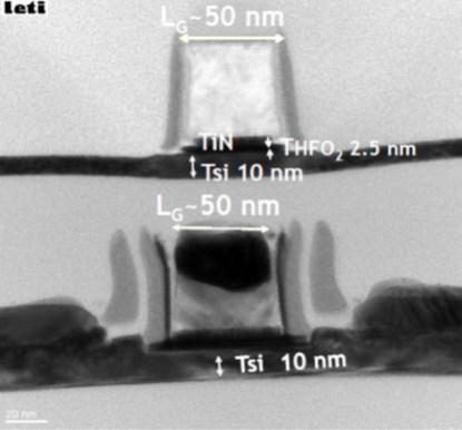
Since before 2009, CEA-Leti has been busy working on processing flows to enable monolithic 3D devices. Perrine Batude won the 2009 Roger A. Haken Best Student Paper Award for the IEDM 2009 paper "Advances in 3D CMOS Sequential Integration" (subscription required). In that paper, she and her co-authors showed results for a sequentially processed P over N (no metal between transistor layers) test chip. In an IEDM 2011 paper, she and her colleagues showed a 50nm 3D sequential structure on 10nm channel silicon, illustrated below.
Faynot was also asked if stress is a big issue. He replied that stress is not an issue. Rather, the biggest challenges are integration ones.
Leti has a PDK ready to go for those who want to design a test circuit in their monolithic 3D flow. The company has ELDO, HSPICE, Calibre, StarRC, and other files available, and it has said that monolithic 3D offers savings of at least 55% on area, 23% on performance, and 25% on power over 2D.
Not too surprisingly, the Qualcomm logo showed up on some of the Leti presentation slides. Back in December, Leti signed an agreement to work with Qualcomm. ST and IBM have also been working with Leti in various areas.
Since before 2009, CEA-Leti has been busy working on processing flows to enable monolithic 3D devices. Perrine Batude won the 2009 Roger A. Haken Best Student Paper Award for the IEDM 2009 paper "Advances in 3D CMOS Sequential Integration" (subscription required). In that paper, she and her co-authors showed results for a sequentially processed P over N (no metal between transistor layers) test chip. In an IEDM 2011 paper, she and her colleagues showed a 50nm 3D sequential structure on 10nm channel silicon, illustrated below.
CEA-Leti also opened a complete 300mm fab extension dedicated to 3D-integration applications -- both parallel and monolithic -- with an inauguration event in January 2011. In December 2013, Soitec and CEA renewed their longstanding partnership for an additional five years.
Clearly, monolithic 3D integration has a very important role for the future of the semiconductor industry. It is therefore fitting that the traditional IEEE conference on SOI has extended its scope and now calls itself S3S: SOI technology, 3D Integration, and Subthreshold Microelectronics. The 2014 S3S Conference is scheduled for Oct. 6-9 at the Westin San Francisco Airport. CEA-Leti will present its work on CMOS monolithic 3D IC. Researchers from MIT and Stanford will present manufacturing monolithic 3D devices with materials other than silicon. With five invited presentations covering topics from design tools to monolithic 3D NAND and other 3D memories, this would be a great opportunity to learn more about monolithic 3D technology.
-- Brian Cronquist is vice president of technology and IP at MonolithIC 3D Inc. He has 35 years of semiconductor industry experience as senior director of technology development and foundry at the nonvolatile FPGA provider Actel (now Microsemi), starting and building Chartered Semiconductor-Singapore (now GlobalFoundries), running startup wafer fab engineering teams at Sierra Semiconductor (now PMC-Sierra), and developing process technology at AMI and Synertek/Honeywell. He has published more than 100 technical papers in the fields of semiconductor microelectronic radiation effects and hardening, as well as new 3D-IC, logic, antifuse, and flash processes, devices, and reliability. He holds more than 60 issued/pending patents.


 RSS Feed