A Must-See Chart from ISSCC2014

Zvi Or-Bach, MonolithIC 3D, & Ben Louie, Zeno Semiconductors
The chart below was presented at ISSCC 2014 by Dinesh Maheshwari, CTO of Memory Products Division at Cypress Semiconductors. The slide clearly illustrates that embedded SRAM ("eSRAM") scaling is broken.
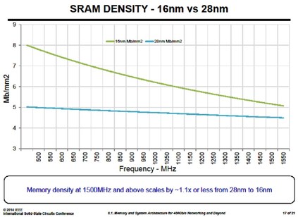
Instead of the expected 4X density improvement for a large memory block with two nodes of scaling, the improvement range is only 1.6X for low performance to 1.1X at good performance. Since eSRAM dominates most SoC silicon area, we have to conclude that dimensional scaling is broken as well. Let’s discuss it further.Instead of the expected 4X density improvement for a large memory block with two nodes of scaling, the improvement range is only 1.6X for low performance to 1.1X at good performance. Since eSRAM dominates most SoC silicon area, we have to conclude that dimensional scaling is broken as well. Let’s discuss it further.
The following slide was presented by Intel at their recent analyst day. It illustrates the impact of dimensional scaling on advanced wafer cost ($/mm²) mostly due to the escalating cost of lithography. Intel believes it can compensate for this exponential wafer cost increase by increasing their transistor density (mm²/transistor) to maintain historical cost reduction of transistor cost ($/transistor).
The following slide was presented by Intel at their recent analyst day. It illustrates the impact of dimensional scaling on advanced wafer cost ($/mm²) mostly due to the escalating cost of lithography. Intel believes it can compensate for this exponential wafer cost increase by increasing their transistor density (mm²/transistor) to maintain historical cost reduction of transistor cost ($/transistor).
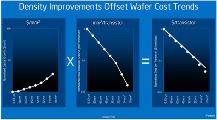
Perhaps it can, but at this time we keep hearing about delays in ramping up the 14nm line. (See "Broadwell Coming, but Not Until the End of the Year.") This reminds us of the famous joke, "Will make it on the volume," since increasing transistor density is directly related to the aggressive dimensional scaling that was driving the escalating wafer cost in the first place.
Most industry players confirm that cost-reduction for transistors has stopped beyond the 28nm process node, as is illustrated by the ASML chart below. This chart was presented at SEMICON West 2013.
Most industry players confirm that cost-reduction for transistors has stopped beyond the 28nm process node, as is illustrated by the ASML chart below. This chart was presented at SEMICON West 2013.
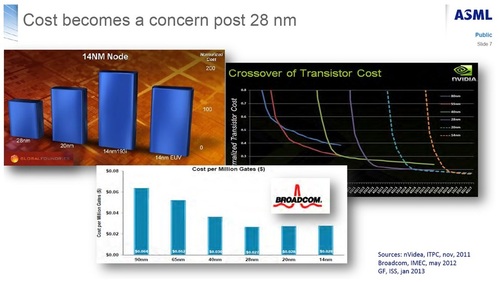
It also clear that EUV is not going to be ready for the 16/14nm node. In fact, most observers are in agreement that EUV will also miss the 10nm node.
For some applications, keeping the cost-per-transistor about the same while reducing power or increasing speed might still justify going to 20nm or 14nm. The IMEC/Cypress chart above indicates that this will not be true for most designs. The fraction of the die area used for eSRAM is consistently growing with scaling, and it already regularly exceeds 50%. The following two charts from Semico, which were recently updated, illustrate this for advanced SoC and average SoC implementations.
For some applications, keeping the cost-per-transistor about the same while reducing power or increasing speed might still justify going to 20nm or 14nm. The IMEC/Cypress chart above indicates that this will not be true for most designs. The fraction of the die area used for eSRAM is consistently growing with scaling, and it already regularly exceeds 50%. The following two charts from Semico, which were recently updated, illustrate this for advanced SoC and average SoC implementations.
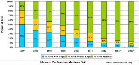
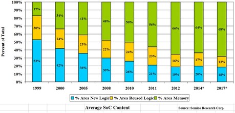
Taking into account that 16/14 nm silicon is almost twice as expensive per unit area as that of 28 nm, this implies that beyond 28nm, SoC costs for the same functionality will escalate for most designs, and this will dampen even further the transition to advanced nodes such as 20nm or 16/14nm!
This clearly seems to indicate a paradigm shift after 50 years of consistent cost-reduction with dimensional scaling. Indications of this were already presented in our blog, Paradigm Shift: Semi Equipment Tells the Future, and in recent news articles such asAnalysis: ASML Stops 450mm Dead and Intel Cancels Fab 42.
Some people will attempt to brush aside Maheshwari's chart shown above, yet multiple sources indicate this is a true new reality that should not be ignored. We first reported it in our blog on ASML at Semicon West 2013, SRAM Scaling Has Stopped, which was backed up by the following IMEC chart as reported in Status Update on Logic and Memory Roadmaps.
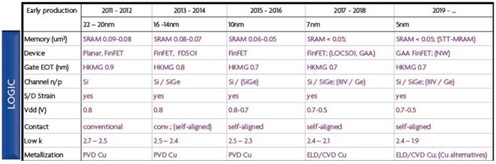
This IMEC chart shows that the reduction of eSRAM bitcell area below 28nm is much less than the 50% expected size-reduction per technology node.
Furthermore, TSMC reported at IEDM 2013 that their bitcell for 16nm is 0.07µm2, and at ISSCC2014 Samsung presented similar results for 14nm finFETs as shown in the following slide.
Furthermore, TSMC reported at IEDM 2013 that their bitcell for 16nm is 0.07µm2, and at ISSCC2014 Samsung presented similar results for 14nm finFETs as shown in the following slide.
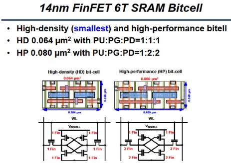
It appears that the TSMC and Samsung bit cell sizes are in line with the IMEC table presented above. It also appears that these trends become even worse when comparing the size of high performance block RAM between technology nodes as presented by Maheshwari.
In the case of block RAM, additional aspects need to be taken into consideration, such as the die size impacts required for implementing a new technology such as finFET. In its ISSCC 2014 paper, Samsung identified complications involved with the transition from planar to finFET, such as quantized width, strong PMOS, and a lack of the body-bias effect. Samsung disclosed a die size impact of 0.87% in order to add a Disturbance Noise Reduction (DNR) scheme to deal with its larger, more stable High Performance (HP) bit-cell. Samsung did not disclose the area impact of its proposed Negative Bitline write assist scheme used with their high density HD bit-cell, but we can assume it is likely significantly larger than the proposed scheme for the HP bit-cell.
Some of the issues that are holding back scaling eSRAM were presented in our recent blog: The Most Expensive SRAM in the World -- 2.0. Bitcell scaling is getting harder, much harder, and even more so is the ability to scale large blocks of embedded SRAM. When we add the fact that the amount of embedded memory is growing faster than the amount of logic cells, one can predict dark clouds for SoC scaling beyond 28nm. It seems that brute-force scaling is simply not practical anymore, but two technology innovations could solve the SRAM memory scaling problem and provide a scalable high density memory if adopted soon by the industry.
The first innovation is the One-Transistor SRAM (1T SRAM) developed by Zeno Semiconductor. This 1T SRAM utilizes an existing fab process, provides a 90% bitcell size reduction versus conventional 6T SRAM, and it will keep scaling beyond 28nm. The second innovation is that of monolithic 3D, which enables a very effective heterogeneous integration scheme, thereby allowing for the SRAM layer to be optimized for memory while the logic layer can be optimized for logic. (See Monolithic 3D eDRAM on Logic.)
So, what do you think? Do you still believe that traditional scaling is the way to go? Or do you think that we will need to rely on new technologies like 1T-SRAM and monolithic 3D in order to maintain the pace of SoC development?


 RSS Feed