 | We have a guest contribution today from Brian Cronquist, MonolithIC 3D Inc.'s VP of Technology & IP. Brian discusses about monolithic 3d technology as the solution for future scaling as proposed by CEA-Leti. |
Hughes Metras, Leti’s VP of Strategic Partnerships North America, introduced the lead talk at their SemiconWest 2014 Leti Day about monolithic 3D technology as the “solution for scaling.” Hughes presented the Leti device technology roadmap which showed monolithic 3D (M3D) as an alternative to scaling from the 2Xnm nodes to well past 5nm. Here’s the important piece of that roadmap, which highlights the partnership with Qualcomm (ST and IBM helped with some of the work as well):
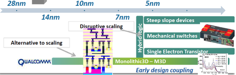
The lead talk was given by device scientist Olivier Faynot, Leti’s Device Department Director. He titled his talk “M3D, a disruptive approach for further scaling,” and began with why the industry needs a solution for scaling.
Most in the industry are in agreement that scaling past the 22nm node, while still quite technically feasible, has priced itself out of most markets. Olivier discussed the what (transistor costs are no longer decreasing) and the why (litho cost escalation and connectivity inefficiencies of energy and delay). And then he made the statement: “if we just keep the current (2Xnm) technology, we can go farther in cost scaling.” [note: see the following blogs and comments for more info on this crucial topic: Tech Design Forums summary "3D and EDA need to make up for Moore’s Law, says Qualcomm" and Zvi-Or-Bach’s EETimes blogs Qualcomm Calls for Monolithic 3D IC and 28nm - The Last Node of Moore's Law.]
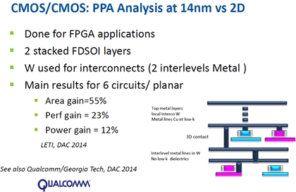
Oliver showed a summary of a DAC2014 paper and a Qualcomm/GeorgiaTech DAC2014 paper Power/Performance/Area analysis of M3D for an FPGA:
Most in the industry are in agreement that scaling past the 22nm node, while still quite technically feasible, has priced itself out of most markets. Olivier discussed the what (transistor costs are no longer decreasing) and the why (litho cost escalation and connectivity inefficiencies of energy and delay). And then he made the statement: “if we just keep the current (2Xnm) technology, we can go farther in cost scaling.” [note: see the following blogs and comments for more info on this crucial topic: Tech Design Forums summary "3D and EDA need to make up for Moore’s Law, says Qualcomm" and Zvi-Or-Bach’s EETimes blogs Qualcomm Calls for Monolithic 3D IC and 28nm - The Last Node of Moore's Law.]
Oliver showed a summary of a DAC2014 paper and a Qualcomm/GeorgiaTech DAC2014 paper Power/Performance/Area analysis of M3D for an FPGA:
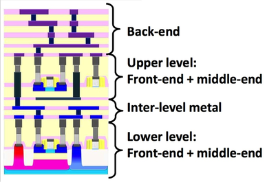
The solution is to build the stack sequentially, in a monolithic fashion. Olivier described their monolithic 3D, or sequential 3D, process flow where the lower-level (first layer) of transistors and its interconnect are conventionally made, then inter-level metal is crafted to help the vertical interconnection, and then a second layer of monocrystalline silicon is layer transferred and oxide-oxide low temperature bonded to the top of the inter-level metal dielectric. This is a blanket layer so there are no alignment issues such as those suffered by the thick layer and pre-made (TSV) parallel processing flows. The layer that is transferred in M3D is very thin (10-200nm final), so that direct alignment thru that thin layer to the lower level alignment marks can be made with conventional equipment and achieve conventional alignment tolerances (single digit nanometers).
Now upper-level transistors are formed utilizing SPER (Solid Phase Epitaxial Regrow) for junction doping at 475-600°C and other lower (<400°C) temperature processing for gate stacks, etc. The upper-level and inter-level vertical interconnect is then processed, again with full alignment capability to the lower layer. Note that the lower level transistor Ni salicides are stabilized with platinum co-deposition and fluorine/tungsten implantation to enable their survival at the 475-600°C SPER thermal exposure.
Now upper-level transistors are formed utilizing SPER (Solid Phase Epitaxial Regrow) for junction doping at 475-600°C and other lower (<400°C) temperature processing for gate stacks, etc. The upper-level and inter-level vertical interconnect is then processed, again with full alignment capability to the lower layer. Note that the lower level transistor Ni salicides are stabilized with platinum co-deposition and fluorine/tungsten implantation to enable their survival at the 475-600°C SPER thermal exposure.
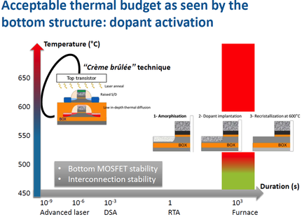
Oliver also talked about using laser annealing to activate implanted dopants and repair damages during upper-level transistor processing. He called the laser (pulsed and short wavelength) option of solving the thermal challenge of monolithic 3D as the “crème brûlée” of methods and they were ‘seeing good results.’ Hopefully we will see published data soon. For more information on SPER and laser processing please see my recent blog Monolithic 3DIC: Overcoming silicon defects.
Oliver was also asked in the Q&A if stress was a big issue. He replied that stress was not an issue, rather, the biggest challenges were integration ones (how to form a low temp top transistor, stability of the local interconnect level, and the bottom transistor salicide stability). Olivier was asked in the Q&A what the observed performance differences were between the upper-level and lower-level transistors. He replied” Currently we are achieving 95% (of the lower for the upper). We believe we can make 100%.”
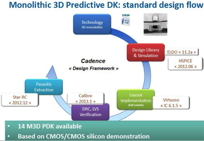
Leti has a 14nmPDK ready to go for those who want to design a test circuit in their monolithic 3D flow. They have ELDO, HSPICE, Virtusoso, Calibre, StarRC, etc. files available.
Leti has a 14nmPDK ready to go for those who want to design a test circuit in their monolithic 3D flow. They have ELDO, HSPICE, Virtusoso, Calibre, StarRC, etc. files available.
Not too surprisingly, the Qualcomm logo showed up on some of the Leti presentation slides. Back in December 2013, Leti signed an agreement to work with Qualcomm – Qualcomm to Evaluate Leti’s Non-TSV 3D Process. ST and IBM have also been working with Leti in various aspects, for example, IBM & Leti used COMPOSE3 to simulate a monolithic InGaAs nFET monolithically over a SiGe pFET on SOI.
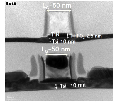
CEA-Leti has been busy working on processing flows to enable monolithic 3D devices since before 2009. Perrine Batude won the 2009 Roger A. Haken Best Student Paper Award for the IEDM 2009 paper entitled, “Advances in 3D CMOS Sequential Integration,” where she showed results for a sequentially processed P over N (no metal between transistors layers) testchip Batude’s 2011 IEDM paper showed a 50nm 3D sequential structure on 10nm channel silicon:
CEA-Leti has been busy working on processing flows to enable monolithic 3D devices since before 2009. Perrine Batude won the 2009 Roger A. Haken Best Student Paper Award for the IEDM 2009 paper entitled, “Advances in 3D CMOS Sequential Integration,” where she showed results for a sequentially processed P over N (no metal between transistors layers) testchip Batude’s 2011 IEDM paper showed a 50nm 3D sequential structure on 10nm channel silicon:
CEA-Leti also opened a complete 300mm fab extension dedicated to 3D-integration applications, both parallel and monolithic, with an inauguration event in January 2011. As well, back in December 2013, Soitec and CEA renewed their long-standing partnership for an additional five years.
Clearly, monolithic 3D integration has a very important role for the future of the semiconductor industry. I would like to invite you to the IEEE S3S Conference: SOI technology, 3D Integration, and Subthreshold Microelectronics. The 2014 S3S Conference will be held October 6-9, 2014 at the Westin San Francisco Airport. This would be a great opportunity to learn more about monolithic 3D technology, with five invited presentations covering topics from design tools to monolithic 3D NAND and other 3D memories. CEA Leti will present their work on CMOS monolithic 3D IC. Researchers from MIT and Stanford will present manufacturing monolithic 3D devices with materials other than silicon.
See you there!


 RSS Feed