
We have a guest contribution from Zvi Or-Bach, the President and CEO of MonolithIC 3D Inc. Mr. Or-Bach discusses about the shift in semi equipment, a paradigm confirmed lately.
Our blog Paradigm shift: Semi equipment tells the future, was focused on the quote: “Now more money is spent on upgrading existing facilities, while new capacity additions are occurring at a lower pace.” And now, just prior to Semicon West, we have the conclusion of the recent SEMI’s World Fab Forecast — Technology Node Transitions Slowing Below 32 nm. The SEMI World Fab Forecast uses a bottom-up approach methodology, providing high-level summaries and graphs, and in-depth analyses of capital expenditures, capacities, technology and products by fab. The following chart illustrates this new paradigm:
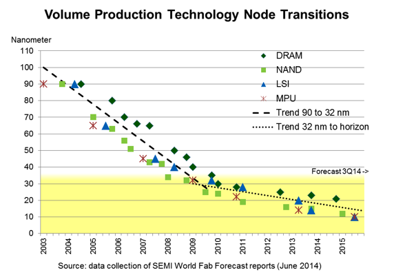
The report states: “The cost per wafer has become an increasing concern below the 32nm node. The expected cost reduction benefit of production at smaller nodes is diminishing and is not keeping pace with the scaling benefits in many cases. This has widespread and fundamental implications for an industry long following the cadences of Moore’s Law… These may be contributing factors as to why some volume fabs are exhibiting a lag in beginning production of new technology node. Now evident quantitatively for the first time, there is evidence of a clear slowdown in volume production scaling of leading technology node transitions.” (emphasis added)
It is fitting to point to the comment made to EE Times coverage on Semicon West – 13 Things I Heard at Semicon West: “No matter what Intel says, Moore’s Law is slowing down,” said Bob Johnson, a semiconductor analyst for Gartner. “Only a few high-volume, high-performance apps can justify 20 nm and beyond.” He sees problems ahead for logic chips in general,” and to follow with quotes from another EE Times article – Silicon Highway Narrows, Twists: “Most foundries have yet to start buying the capital equipment needed for the 14/16 nm node, which for many will be the first to support FinFETs, says Trafas of KLA-Tencor. Gear companies hope the orders start coming in the fall…Indeed, he says, one of the big questions many capital equipment execs will bring to this year’s Semicon West event on July 7 is, “When will the 16/14 nm investments begin?”
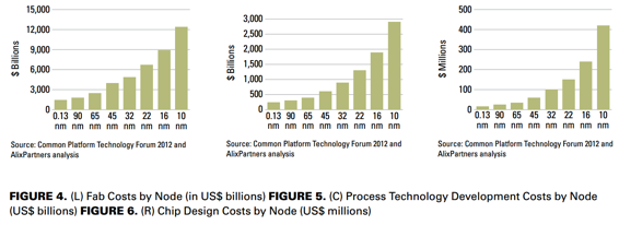
Since the 65 nm node, escalating costs of fab and process technology development and design, as illustrated in the chart below, put a huge pressure on the industry.
It is fitting to point to the comment made to EE Times coverage on Semicon West – 13 Things I Heard at Semicon West: “No matter what Intel says, Moore’s Law is slowing down,” said Bob Johnson, a semiconductor analyst for Gartner. “Only a few high-volume, high-performance apps can justify 20 nm and beyond.” He sees problems ahead for logic chips in general,” and to follow with quotes from another EE Times article – Silicon Highway Narrows, Twists: “Most foundries have yet to start buying the capital equipment needed for the 14/16 nm node, which for many will be the first to support FinFETs, says Trafas of KLA-Tencor. Gear companies hope the orders start coming in the fall…Indeed, he says, one of the big questions many capital equipment execs will bring to this year’s Semicon West event on July 7 is, “When will the 16/14 nm investments begin?”
Since the 65 nm node, escalating costs of fab and process technology development and design, as illustrated in the chart below, put a huge pressure on the industry.
These escalating costs drove consolidation in the industry, cutting down to a handful the vendors who are still pursuing the leading edge.
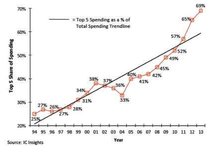
At the recent (2014) SST ConFab in Las Vegas Bill McClean shared his annual report on Major trends shaping the future IC Industry. Bill reports: “Over the last two decades, the percentage of capex being spent by the top 5 has steadily increased to its current 70% with the big three of Samsung, Intel and TSMC being responsible for over 50%.” This is illustrated by the following chart.
At the recent (2014) SST ConFab in Las Vegas Bill McClean shared his annual report on Major trends shaping the future IC Industry. Bill reports: “Over the last two decades, the percentage of capex being spent by the top 5 has steadily increased to its current 70% with the big three of Samsung, Intel and TSMC being responsible for over 50%.” This is illustrated by the following chart.
Clearly the escalating costs drove out most but the largest vendor, but now we are facing the ”second punch” – the diminishing returns.
In the recent ITC conference Harry J. Levinson of GlobalFoundries in his talk: Lithography Issues for High Volume Manufacturing” presented the following chart:
In the recent ITC conference Harry J. Levinson of GlobalFoundries in his talk: Lithography Issues for High Volume Manufacturing” presented the following chart:
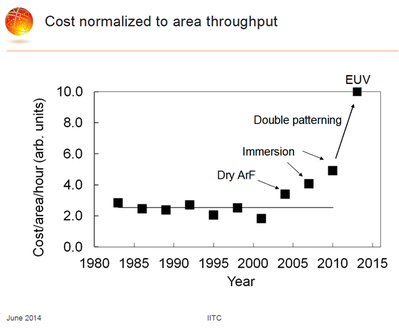
The dramatic increase of lithography cost eats away the historical transistor cost reduction resulting from reduced dimensions, as we reported in our blog Qualcomm: Scaling down is not cost-economic anymore – so we are looking at true monolithic 3D. Quoting Qualcomm “One of the biggest problems is cost. We are very cost sensitive. Moore’s Law has been great. Now, although we are still scaling down it’s not cost-economic anymore. It’s creating a big problem for us.” Accordingly we detailed in our blog that Moore’s Law has stopped at 28nmand following nodes would not provide lower transistor cost, and for most application will result in higher SoC costs.
We should not be surprised that the production ramp up below 28 nm is extremely slow. There is too much money involved to put it into the wrong place.
Going back to the SEMI World Fab Forecast, the authors ask “What’s next?” and respond: “Many in our industry are grappling with what to do as they have perceived the coming slowdown in technology node transitions. IC manufacturers are now increasingly looking outside of conventional lithography and wafer size scaling approaches to pick up the pace of cost reduction while increasing transistor density and performance. Using memory as an example, to cope with increasing challenges in continuing to scale 2D, memory companies are looking into 3D.”
So the memory vendors already started shifting their Capex budget to scaling up with 3D NAND, instead of scaling to smaller dimension. Recently Qualcomm announced their collaboration with SMIC – China’s SMIC-Qualcomm 28-nm Deal: Why Now? – indicating more capacity build-up for 28 nm with looking forward to scaling up with monolithic 3D for logic as well. Quoting: ”Going forward, SMIC will also extend its technology offerings on 3DIC and RF front-end wafer manufacturing in support of Qualcomm”.
It is clear now that we are seeing a paradigm shift in the semiconductor equipment industry. After many decades of relentless dimensional scaling every two years, there is a change coming and we see a lower rate of dimensional scaling and exploration of other paths, to keep industry’s march on. We do believe that the next few decades will be about scaling with 3D Integration and we are pleased to see many others thinking the same.
The 2014 S3S Conference is scheduled for October 6-9, 2014, at the Westin San Francisco Airport, and would be a great opportunity to learn more about monolithic 3D technology, with five invited presentations covering topics from design tools to monolithic 3D NAND and other 3D memories. CEA Leti will present their work on CMOS monolithic 3D IC. Researchers from MIT and Stanford will present manufacturing monolithic 3D devices with materials other than silicon.


 RSS Feed