Monolithic 3D Inc., the Next Generation 3D-IC Company
  • Home
  • Technology
    • Technology
    • Papers, Presentations and Patents
    • Overview >
      • Background
      • Why Monolithic 3D?
      • Paths to Monolithic 3D
      • Applications
    • Ion-Cut: The Building Block
    • Monolithic 3D Logic >
      • RCAT
      • HKMG
      • Laser Annealing
      • RCJLT
      • 3D Embedded RAM
      • 3D Gate Array
      • FPGA
      • Ultra Large Integration - Redundancy and Repair
    • Monolithic 3D Memory >
      • 3D DRAM
      • 3D Resistive Memories
      • 3D Flash
    • Monolithic 3D Electro-Optics >
      • 3D Image Sensors
      • 3D Micro-Displays
  • 3D-IC Edge
    • 3D-IC Edge
  • News & Events
    • News & Events
    • S3S15 Game Change 2.0 Video/P
    • Webcast
    • Webinar
    • Press Releases
    • In the News
    • Upcoming Events
  • About Us
    • About Us
    • History
    • Team
    • Careers
    • Contact Us
  • Blog
  • Simulators

Scaling makes monolithic 3D IC practical

10/22/2013

0 Comments

 
Picture
We have a guest contribution from Zvi Or-Bach, the President and CEO of MonolithIC 3D Inc. Zvi's blog post is about the scaling process that makes monolithic 3D IC practical.

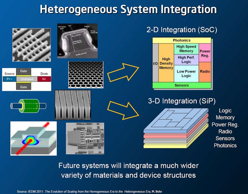
In the 1960s, James Early of Bell Labs proposed three-dimensional structures as a natural evolution for integrated circuits. Since then many attempts have been made to develop such a technology. So far, none have been able to overcome the 400°C process temperature limitation imposed by the use of aluminum and copper in modern IC technologies for the underlying interconnects without great compromises. The “Holy Grail” of 3D IC has been the monolithic 3D, also known as sequential 3D, where a second transistor layer could be constructed directly over the base wafer using ultra-thin silicon – less than 100nm – thus enabling a very rich vertical connectivity.

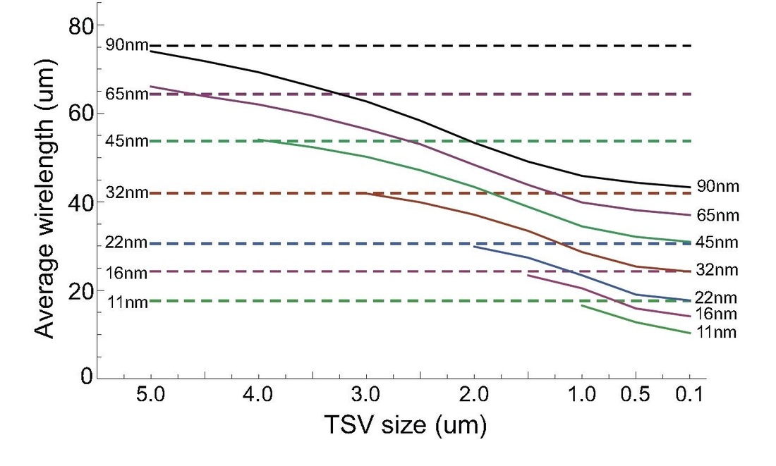
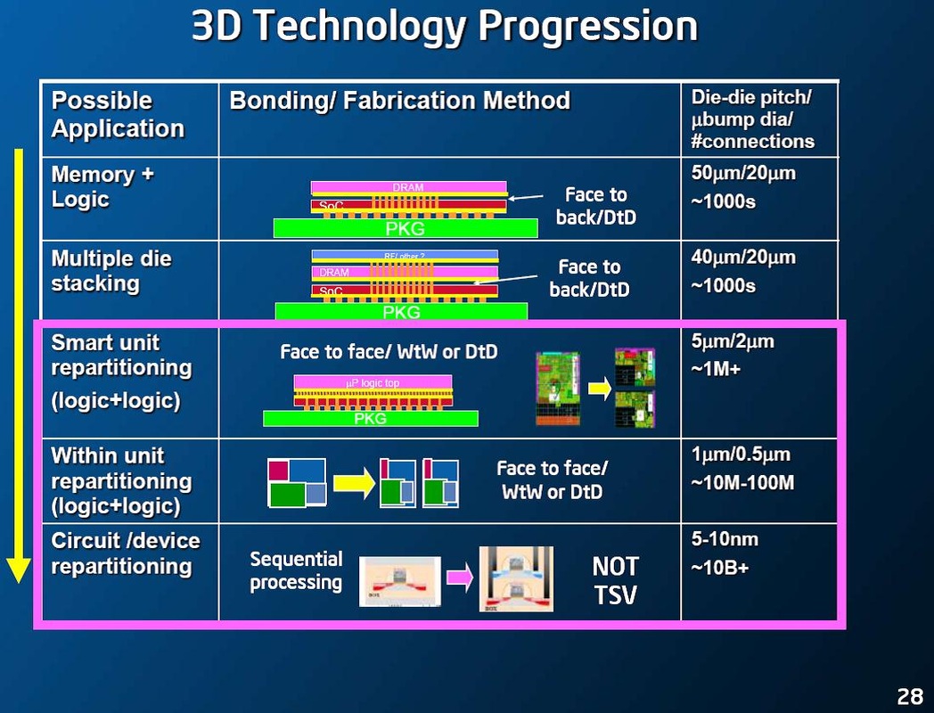
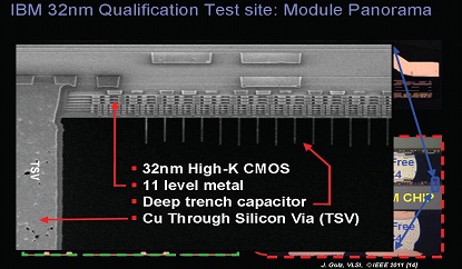
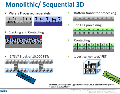
Accordingly the industry developed a 3D IC technology based on TSV (Thru Silicon Via) where each strata (wafer) could be independently processed, then after thinning at least one wafer, place in a 3D configuration, and then connect the strata with TSV using a low temperature  (<400°C) process. This independent (parallel) processing has its own advantages; however, the use of thick layers (>50 µm) greatly limits the vertical connectivity, requires development of all new processing flows, and is still too expensive for broad market adoption. On the other hand, monolithic 3D IC provides a 10,000x better vertical connectivity and would bring many additional benefits as was recently presented in the IEEE 3D IC conference.

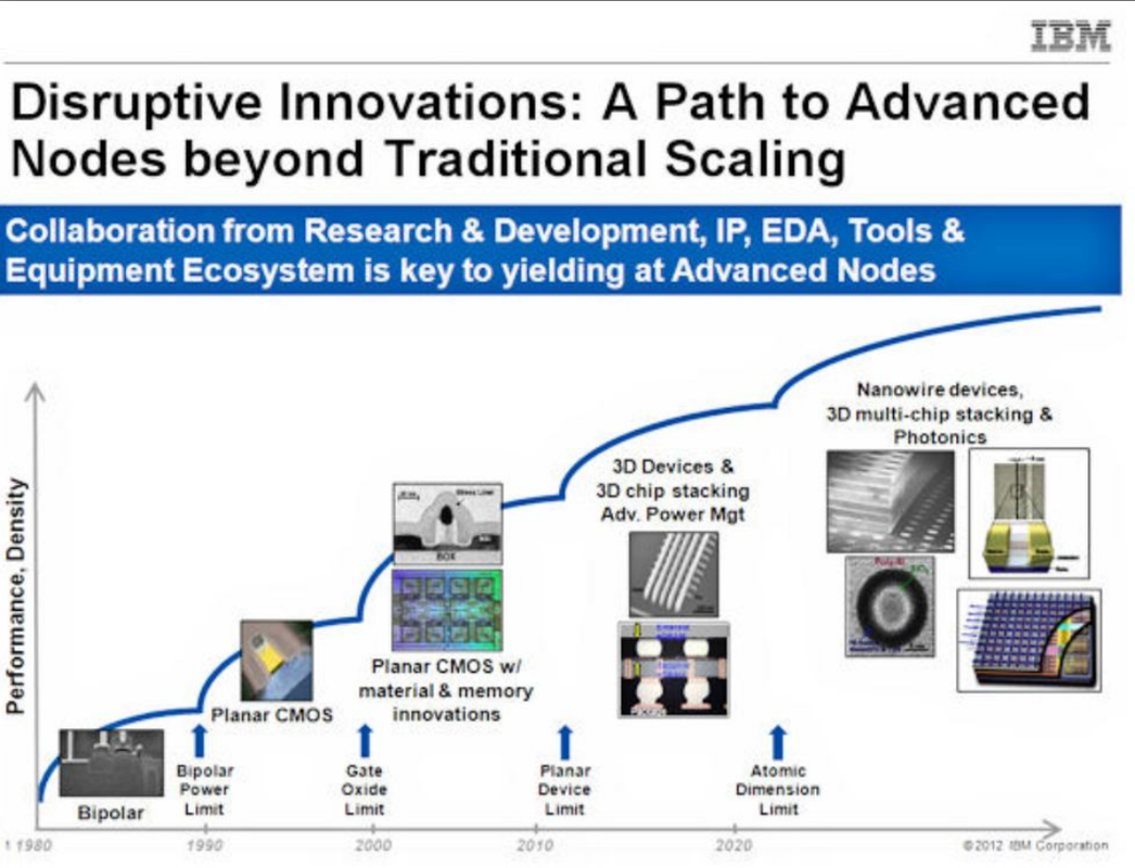
The semiconductor industry is always on the move and new technologies are constantly being introduced making changes the only thing that is constant. For the most part dimensional scaling has been associated with introducing new materials and challenges, thereby making process steps that were once easy far more complex and difficult. But not so in respect to monolithic 3D IC.

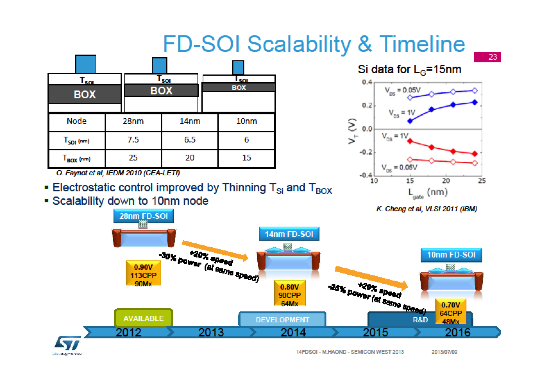
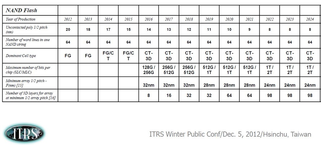
The amount of silicon associated with a transistor structure was measured in microns in the early days of the IC industry and has now scaled down to the hundreds and the tens of nano-meters. The new generation of advanced transistors have thicknesses in nanometers as is illustrated in the following ST Micro slide.

Picture
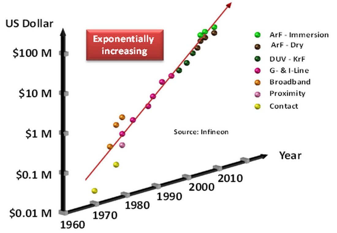
Dimensional scaling has also brought down the amount of time used for transistor activation/annealing, to allow sharper transistor junction definition, as illustrated in the following Ultratech slide
Picture
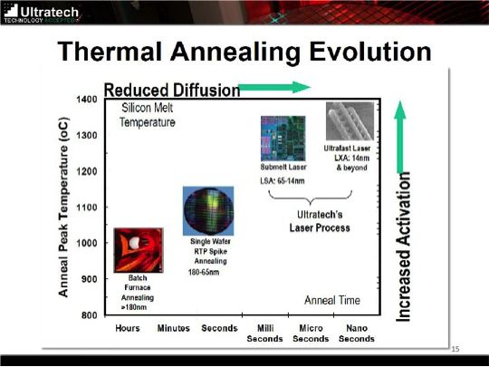
Clearly the amount of heat associated with transistor formation has reduced dramatically with scaling as less silicon gets heated for far less time.

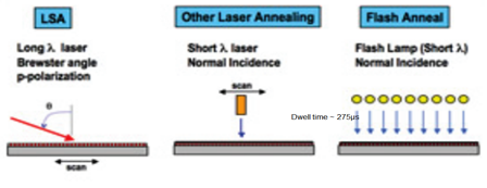
And unlike furnace heating or RTP annealing, with laser annealing the heat is coming from the top and directed only on small part of the wafer as illustrated below.

Picture
Picture
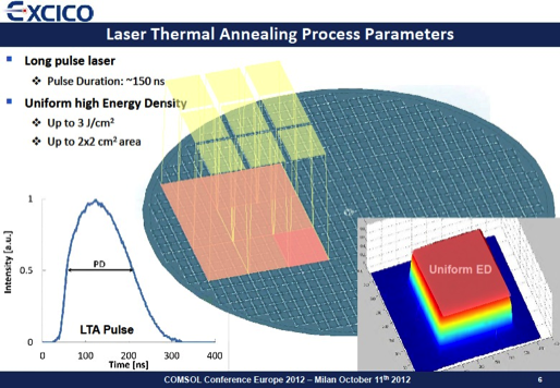
The following illustrates Excico pulsed excimer laser which can cover 2×2 cm2 of the wafer.
Picture
Worth noting that this week we learned of good results when utilizing Excico laser annealing for 3D memory enhancement – Laser thermal anneal to boost performance of 3D memory device.

These trends help make it practical to protect the first strata interconnect from the high temperature process required for the second strata transistor formation. As the high temperature is on small amount of silicon for a very short time and for a small part of the wafer, the total amount of thermal energy required for activation/annealing is now very small.

One of the three most newsworthy topics and papers included in the 2013 IEDM Tip Sheet for the “Advances in CMOS Technology & Future Scaling Possibilities” track was a monolithic 3D chip fabricated using a laser (reported by Solid State magazine “Monolithic 3D chip fabricated without TSVs“). Quoting: “To build the device layers, the researchers deposited amorphous silicon and crystallized it with laser pulses. They then used a novel low-temperature chemical mechanical planarization (CMP) technique to thin and planarize the silicon, enabling the fabrication of ultrathin, ultraflat devices. The monolithic 3D architecture demonstrated high performance – 3-ps logic circuits, 1-T 500ns nonvolatile memories and 6T SRAMs with low noise and small footprints, making it potentially suitable for compact, energy-efficient mobile products.”

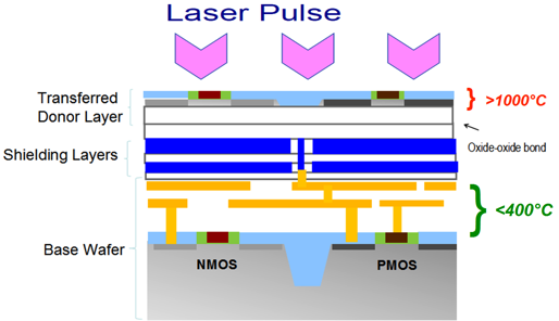
Furthermore, in last two weeks we presented in the IEEE 3D IC and IEEE S3S conferences an alternative simulation based work. We suggested to use a smart-cut® for the formation of the second strata (and not amorphous silicon crystallization) with innovative shielding layers to protect the first strata interconnect, as illustrated below.

Picture
Currently there are at least three different laser annealing systems offered on the market. The shielding layers could be adjusted according to the preferred choice of the laser annealing system. Our simulations show that if an excimer laser such as one offered by Excico is used, then even without these shielding layers the first strata routing layers are not adversely impacted by the laser annealing process.

Summary: In short, dimensional scaling is becoming harder and yet it makes monolithic 3D easier. We should be able to keep scaling one way or the other (or even both), and keep enjoying the benefits.

Note: smart-cut® s a register TM of Soitec

submit to reddit
0 Comments

3D-IC: Two for one

9/26/2013

0 Comments

 
Picture
We have a guest contribution from Zvi Or-Bach, the President and CEO of MonolithIC 3D Inc. Zvi details MonolithIC 3D Inc's participation at the upcoming events in 3D IC field and the key role of the company in each event. 

This coming October there are two IEEE Conferences discussing 3D IC, both are within an easy drive from Silicon Valley.

The first one is the IEEE International Conference on 3D System Integration (3D IC), October 2-4, 2013 in San Francisco, and just following in the second week of October is the S3S Conference on October 7-10 in Monterey. The IEEE S3S Conference was enhanced this year to include the 3D IC track and accordingly got the new name S3S (SOI-3D-Subthreshold). It does indicate the growing importance and interest in 3D IC technology.

This year is special in that both of these conferences will contain presentations on the two aspects of 3D IC technologies. The first one is 3D IC by the use of Through -Silicon-Via which some call -”parallel” 3D and the second one is the monolithic 3D-IC which some call “sequential.”

This is very important progress for the second type of 3D IC technology. I clearly remember back in early 2010 attending another local IEEE 3D IC Conference: 3D Interconnect: Shaping Future Technology. An IBM technologist started his presentation titled “Through Silicon Via (TSV) for 3D integration” with an apology for the redundancy in his presentation title, stating that if it 3D integration it must be TSV!

 Yes, we have made quite a lot of progress since then. This year one of the major semiconductor research organization – CEA Leti – has placed monolithic 3D on its near term road-map, and was followed shortly after by a Samsung announcement of mass production of monolithic 3D non volatile memories – 3D NAND.

We are now learning to accept that 3D IC has two sides, which in fact complement each other. In hoping not to over-simplify- I would say that main function of the TSV type of 3D ICs is to overcome the limitation of PCB interconnect as well being manifest by the well known Hybrid Memory Cube consortium, bridging the gap between DRAM memories being built by the memory vendors and the processors being build by the processor vendors. At the recent VLSI Conference Dr. Jack Sun, CTO of TSMC present the 1000x gap which is been open between  on chip interconnect and the off chip interconnect. This clearly explain why TSMC is putting so much effort on TSV technology – see following figure:

Picture
Figure 1: System level interconnect gaps
On the other hand, monolithic 3D’s function is to enable the continuation of Moore’s Law and to overcome the escalating on-chip interconnect gap. Quoting Robert Gilmore, Qualcomm VP of Engineering, from his invited paper at the recent VLSI conference: “As performance mismatch between devices and interconnects increases, designs have become interconnect limited. Monolithic 3D (M3D) is an emerging integration technology that is poised to reduce the gap significantly between device and interconnect delays to extend the semiconductor roadmap beyond the 2D scaling trajectory predicted by Moore’s Law…” In IITC11 (IEEE Interconnect Conference 2011) Dr. Kim presented a detailed work on the effect of the TSV size for 3D IC of 4 layers vs. 2D. The result showed that for TSV of 0.1µm – which is the case in monolithic 3D – the 3D device wire length (power and performance) were equivalent of scaling by two process nodes! The work also showed that for TSV of 5.0µm – resulted with no improvement at all (today conventional TSV are striving to reach the 5.0µm size) – see the following chart:
Picture
Figure 2: Cross comparison of various 2D and 3D technologies. Dashed lines are wirelengths of 2D ICs. #dies: 4.
So as monolithic 3D is becoming an important part of the 3D IC space, we are most honored to have a role in these coming IEEE conferences. It will start on October 2nd in SF when we will present a Tutorial that is open for all conference attendees. In this Monolithic 3DIC Tutorial we plan to present more than 10 powerful advantages being opened up by the new dimension for integrated circuits. Some of those are well known and some probably were not presented before. These new capabilities that are about to open up would very important in various market and applications.

In the following S3S conference we are scheduled on October 8, to provide the 3D Plenary Talk for the 3D IC track of the S3S conference. The Plenary Talk will present three independent paths for monolithic 3D using the same materials, fab equipment and well established semiconductor processes for monolithic 3D IC. These three paths could be used independently or be mixed providing multiple options for tailoring differently by different entities.

Clearly 3D IC technologies are growing in importance and this coming October brings golden opportunities to get a ‘two for one’ and catch up and learn the latest and greatest in TSV and monolithic 3D technologies — looking forward to see you there.

submit to reddit
0 Comments

MonolithIC 3D Inc. at 2013 S3S Conference

9/17/2013

0 Comments

 
Picture


Join MonolithIC 3D Inc. at the IEEE SOI-3D-Subthreshold Microelectronics Technology Unified Conference on October 7th thru 10th, 2013 in Monterey, CA. The conference will start with three plenary talks, one for each of the conference tracks. We are most honored for being invited to give the 3D Plenary Talk. Our thanks to the organizing committee for their invitation.  We are pleased to see monolithic 3D technology is rapidly becoming part of the 3D IC field. MonolithIC 3D Inc. will be represented by Zvi Or-Bach, President and CEO of the company.

The 3D Plenary Talk will describe “Practical Process Flows for Monolithic 3D”. In this session Mr. Or-Bach will present three approaches to obtain 3D logic ICs. You can access the Technical Program of the Conference here.

Zvi Or-Bach: “Monolithic 3D ICs provides a practical short term path to keep the semiconductor industry on track with Moore's Law as dimensional scaling is reaching its diminishing return phase. Monolithic 3D IC allows the existing industry infrastructure and silicon knowledge to be utilized while research activities continue the search for other alternatives. It should be mentioned that we are also honored to be giving a tutorial on monolithic 3D at the IEEE 3D System Integration Conference on Oct 2-4, 2013, in San Francisco. At the tutorial we plan to present the many significant additional benefits that are available with monolithic 3D IC."

The three approaches which will be presented at S3S for monolithic 3D ICs are:

RCAT – Process the high temperature on a generic structure prior to layer transfer , and finish with cold processes; i.e., etch & depositions.

Gate Replacement (Gate Last HKMG) – Process the high temperature on a repeating structure prior to layer transfer, and finish with 'gate replacement' cold processes.

Laser Annealing – Use short laser pulses to locally heat and anneal the top layer while protecting the interconnection layers below from the topside heat.

In addition, the company will also present at the poster session the thermal compatibility of laser annealing of newly built 3D structures with transistors and interconnect circuits lying beneath in “Thermal Considerations for Monolithic Integration of Three-Dimensional Integrated Circuits”. This work was done in collaboration with the Department of Electrical Engineering, IIT-Bombay, India.

Abstract of poster: A major consideration for practical integration of 3D integrated circuits is compatibility of the thermal processes used to build new transistors in the vertical dimension, with sustained viability of the devices already fabricated beneath. Major contributions to the thermal profile of IC processes are laser-based anneals, rapid-thermal anneals and deposition processes, and traditional furnace processes for both annealing and film deposition. In this work, we consider the thermal compatibility of laser annealing of newly built 3D structures, with the ICs lying beneath.

Please join us at the 2013 S3S Conference held this year in Monterey, CA October 7th thru 10th, 2013. Here you can find the registration link and fee information to attend the conference.

submit to reddit
0 Comments

MonolithIC 3D Inc. at IEEE International Conference on 3D System Integration (3D IC)

9/10/2013

0 Comments

 
Picture
Join MonolithIC 3D Inc. at IEEE International Conference on 3D System Integration (3D IC) on October 2nd -4th, 2013 in San Francisco, CA. Zvi Or-Bach, President and CEO of MonolithIC 3D Inc. will present a guest tutorial on 3D IC edge. The company will also give the presentation: “Pulsed Laser Annealing: A scalable and practical technology for monolithic 3D IC” in session VII of the event. You can access the Technical Program of the Conference here.

Zvi Or-Bach, President and CEO of MonolithIC 3D Inc. will be featured as guest speaker to present a tutorial on Monolithic 3D IC. The tutorial describes the advantages of monolithic 3d as an alternative to maintain the exponential increase in integration. Some of the advantages of this technology include reductions of cost, decreases in power consumption, and improvements in performance, and bring some new and compelling benefits like:
  • Continuing reductions in die size and power, 
  • Significant advantages for reusing the same fab line and design tools,
  • Heterogeneous Integration
  • Processing multiple layers simultaneously, offering multiples of cost improvement
  • Logic redundancy, allowing 100x integration at good yields
  • Modular Platforms

“Monolithic 3D is a disruptive semiconductor technology. It builds on the existing infrastructure and know-how, and could bring to the high tech industry many more years of continuous progress. While it provides the advantages that dimensional scaling once provided, monolithic 3D offers many more options and benefits. And the best of all is that it could be done in conjunction with dimensional scaling. Now that monolithic 3D is practical, it is time to augment dimensional scaling with monolithic 3D-IC scaling.”

Even more, the company will also give a presentation in session VII on a new path for monolithic 3D IC: “Pulsed Laser Annealing: A scalable and practical technology for monolithic 3D IC”. This work was done in collaboration with the Department of Electrical Engineering, IIT Bombay, India.

Abstract of presentation: Classical dimensional scaling faces challenges from growing on-chip interconnect time delays, and escalating lithography costs and layout limitations. In this paper, we present practical integration schemes for developing cost-efficient 3D ICs in a monolithic fashion, which employ fully depleted transistor channels and laser annealing to achieve sharper junction definition.

Join us at the most important event in the 3D IC industry held this year in San Francisco, CA on October 2nd - 4th, 2013. Here you can find the registration link and fee information to attend the conference.
submit to reddit
0 Comments

"Moore's Law Dead by 2022" - Then, Before or .... ?

9/3/2013

1 Comment

 
Picture
We have a guest contribution from Zvi Or-Bach, the President and CEO of MonolithIC 3D Inc. Zvi discusses the EE Times blog piece: Moore's Law Dead by 2022, Expert Says.

“Moore’s Law Dead by 2022” announces EE Times headline reporting Bob Colwell’s keynote at Hot Chips this week. Actual quote: "Moore's Law -- the ability to pack twice as many transistors on the same sliver of silicon every two years -- will come to an end as soon as 2020 at the 7nm node". Collwell told the audience that DARPA “tracks a list of as many as 30 possible alternatives to the CMOS technology that has been the workhorse of Moore's Law …My personal take is there are two or three promising ones and they are not very promising,". Colwell is the Director of DARPA’s Microsystems Technology Office (MTO) and has both visibility and credibility in these matters. In fact, this is not his first time to publicly state the end of Moore's Law -- he did so at  ACM SIGDA and DAC meetings earlier this year. His slide (below) clearly presents the gap between the end of dimensional (Dennard) scaling and the establishment and ramp-up of alternatives to the current silicon based technology.
Picture
Figure 1
The discussion at EE Times remind us that we have "been hearing this for 20 years or more", so why is it different now? Well, even in the crying wolf story the wolf eventually did come! This time the signs are very clear. In fact, one could argue that as far as cost reduction, Moore's Law is already dead. The following ASML chart clearly shows it.
Picture
Figure 2
Taking into account additional information released during the recent Semicon West, it seems that effective cost for most fabless companies might even go higher with future scaling. Even if we ignore the fact that most foundries chose to keep their metal rules at 20nm when going to 14nm node, with the associated end-device cost implications, advanced nodes come with many additional layout restrictions. Those create circuit design and interconnect overheads that eat away a large part of theoretical scaling benefits. Quoting Andrew Kahng: "Constant area-factors allowed prior node scaling to be 2x, however since 2009 the real scaling has been 2E(2/3)x or ~1.6x due to an “IC Design Gap". Add to it the fact that embedded memory SRAM bit cell is expected to barely scale, as shown in the following slide, and end-product costs might go up even for the same SoC complexity! 
Picture
Figure 3
The following chart from Samsung clearly illustrates this dynamics for NAND, but from the above discussion it may be even more true for SoC.
Picture
Figure 4
The issue of cost has very significant implications. For the semiconductor industry Moore's Law is not just a matter of pride: it became one of its fundamental business drivers. In the food industry vendors keep on selling food as it get consumed, clothing and car industry products get worn out or go out of fashion. But in the semiconductor industry old products mostly get displaced by better new products – the upgrades. Imagine what would happen to the major industry players’ stock if they were to update their projections to expect 20% reduction in revenue!!!
And 20% might be a conservative number once the dynamics of the last 30 years would hit a hard stop.
The following Samsung chart is a good illustration of where we are and the choice that at least Samsung has made:
Picture
Figure 5
We can keep on hoping that the wolf will never come, just as it hasn't before. Or we can take action now before 'they comes'.

Samsung, Toshiba and the rest of the NAND industry are already taking action. On the SoC side the challenges are as severe, yet at this point the industry is consumed by the enormous efforts to bring up FinFETs. It may even bring up compound semiconductors (III-V) for the next node (10nm), but then what? At what cost? For what kind of return?

It seems to me that the right moves are:

First, logic design market needs to adopt an alternative to the embedded memory. IBM stated at the recent Common Platform Forum that adopting eDRAM  gave it the equivalent benefit of one node scaling. This was seconded by Intel’s recent announcement of integrating eDRAM with their new Haswell processor - Intel eDRAM attacks graphics in pre-3-D IC days. An even better option would be the one transistor two state memory breakthrough solution recently developed by Zeno Semiconductors. 

Second, logic design needs to follow the NAND industry by developing monolithic 3D technology for SoC and logic products. In a recent blog we reported that CEA Leti has placed Monolithic 3D is now on the roadmap for 2019. We are pleased to announce that we will provide a tutorial on  monolithic 3D as a part of the upcoming IEEE 3D IC Conference  in early October in San Francisco, and we will follow with a plenary talk the following week at the IEEE S3S Conference in Monterey. In these conferences we also plan to present a new practical process flow for monolithic 3D, leveraging industry’s shift to laser annealing. This technology supports 3D technologies we had presented in the past, and can be used independently for new monolithic 3D process flows. We are looking forward to meeting you all there.
submit to reddit
1 Comment

Monolithic 3D is Now in Production: Samsung Starts Mass Producing Industry’s First 3D Vertical NAND Flash

8/19/2013

0 Comments

 
Picture
We have a guest contribution from Zvi Or-Bach, the President and CEO of MonolithIC 3D Inc. Zvi discusses the starts of mass production for the industry's first 3D vertical NAND flash by Samsung.

Samsung announced today (Aug. 6, 2013) the mass production of the industry's first three-dimensional (3D) Vertical NAND (V-NAND) flash memory, which breaks through the current scaling limit for existing NAND flash technology. Achieving gains in performance and area ratio, the new 3D V-NAND will be used for a wide range of consumer electronics and enterprise applications, including embedded NAND storage and solid state drives (SSDs).
Picture
Samsung's new V-NAND offers a 128 gigabit (Gb) density in a single chip, utilizing the company's proprietary vertical cell structure based on 3D Charge Trap Flash (CTF) technology and vertical interconnect process technology to link the 3D cell array. By applying both of these technologies, Samsung's 3D V-NAND is able to provide over twice the scaling of 20nm-class planar NAND flash.
"For the past 40 years, conventional flash memory has been based on planar structures that make use of floating gates. As manufacturing process technology has proceeded to the 10nm-class and beyond, concern for a scaling limit arose, due to the cell-to-cell interference that causes a trade-off in the reliability of NAND flash products. This also led to added development time and costs.

Samsung's new V-NAND solves such technical challenges by achieving new levels of innovation in circuits, structure and the manufacturing process through which a vertical stacking of planar cell layers for a new 3D structure has been successfully develop...
Also, one of the most important technological achievements of the new Samsung V-NAND is that the company's proprietary vertical interconnect process technology can stack as many as 24 cell layers vertically, using special etching technology that connects the layers electronically by punching holes from the highest layer to the bottom. With the new vertical structure, Samsung can enable higher density NAND flash memory products by increasing the 3D cell layers without having to continue planar scaling, which has become incredibly difficult to achieve”

It’s worth mentioning to the point that while the volume production of TSV based 3D IC is keep being pushed out as discussed in a recent blog: EUV vs TSV: Which one will become production ready first?, this announcement indicates that monolithic 3D NAND is biting the forecast by few years as being illustrated by the following 2012 ITRS chart:
Picture
Figure 2
Clearly monolithic 3D is a promising alternative to dimension scaling, as one can read in this Samsung press release. It also abides very well to the low cost objective for mass production products.

Monolithic 3D technology provides multiple unique and powerful advantages as we present on our site under the tab: 3D-IC Edge. Under item 5 we present the unique advantage that was first introduced in 2007, when Toshiba unveiled its Bit Cost Scalable (BiCS) technology. The unique advantage of 3D NAND is the ability to pattern and process multiple layers simultaneously.

This advantage comes very natural for regular layout fabrics such as memory, but it is also available for logic circuits. The driver for this advantage is the escalating costs of lithography in state of the art IC. The following charts illustrate the impact of dimensional scaling on lithography costs.
Picture
Figure 3
Picture
Figure 4
Currently critical lithography steps dominate the end device production costs as been illustrated in the following chart:
Picture
Figure 5
Accordingly, if the critical lithography step could be used once for multiple layers rather than multiple times for each single layer, then the end device cost would roughly be reduced in proportion to the number of layers processed simultaneously. Multiple memory architectures that support such drastic cost reduction has been presented in various conferences and other forums. Few of those had been presented in our blog: The Flash Industry's Direction, and MonolithIC 3D Inc.'s Solution... This dramatic announcement by Samsung comes in less than a week since we posted the blog: Monolithic 3D is now on the roadmap for 2019. It represents the beginning of a new trend for Moore’s Law – scaling up. As the memory segment of the industry shift its R&D budget and its capital equipment budget for scaling up, the shrinking camp supporting dimension scaling would need to pony up this shortage while facing escalating costs of dimension scaling. It is clear to us that the time to investigate various alternatives for scaling up has come, which also abides to the new industry roadmap recently presented.
submit to reddit
0 Comments

Monolithic 3D is now on the Road-Map for 2019

8/12/2013

0 Comments

 
"The Evolution of Scaling from the Homogenous Era to the Heterogeneous Era"
Picture
We have a guest contribution from Zvi Or-Bach, the President and CEO of MonolithIC 3D Inc. Zvi underlines the milestone for monolithic 3D in the semiconductor road map 2019.

In the recent CEA Leti day, that took place as part of Semicon West 2013, Laurent Malier, Leti CEO presented his "A look at the coming Decade".
Slide 15 of the presentation provides Leti vision for CMOS roadmaps as presented here:
Picture
Figure 1
Monolithic 3D is presented on the road-map as the technology to follow 7nm process node.

Early this year we blogged - IEDM 2012: The pivotal point for monolithic 3D ICs, it is quite reassuring to see monolithic 3D now as part of the industry road-map. As we discussed than the memory vendors are already gearing up for volume production of the 3D NAND as reported recently Toshiba to Build Fab for 3D NAND Flash, leveraging monolithic 3D cost reduction advantage. It only makes senses for the CMOS market to follow. Doubters would ask why the industry would introduce new dimension to a road map that has been extremely successful for over 40 years. And the answer is very simple - because it is successful any more. We are all aware that the escalating costs of lithography had diminished transistors cost reduction as illustrated in the following ASML chart
Picture
Figure 2
But even if we ignore these issues we should remember that "Atoms don't scale" (as was phrased by Bernie Meyerson of IBM), and we are quickly approaching these limit as is presented by the following Intel chart:
Picture
Figure 3
And accordingly Mike Mayberry, director of its component research at Intel, said at the very recent IMEC Technology Forum "...has looked down the highway of conventional silicon development and reckons things become foggy beyond about the 7-nm node".
In fact Mike in his March 2013 presentation titled "Pushing Past the frontiers of Technology" clearly also present the monolithic 3D on his road map as the following slides illustrates
Picture
Figure 4
Picture
Figure 5
As was very well stated by Mark Bohr - Senior Fellow of Technology and Manufacturing Group and a Director of Process Architecture and Integration of Intel:
"The Evolution of Scaling from the Homogenous Era to the Heterogeneous Era"
submit to reddit
0 Comments

“Atoms Don’t Scale”=> What is Beyond 7nm (2019)?                                                               MonolithIC 3D™ - the Future of Semiconductor Scaling

7/23/2013

0 Comments

 
Picture
We have a guest contribution today from Brian Cronquist, MonolithIC 3D Inc.'s VP of Technology & IP. Brian discusses about MonolithIC 3D Inc.'s participation at Semicon West 2013.

Thanks to everybody who came by poster exhibition at the Silicon Innovation Forum at SemiconWest 2013 [SemiWest]! We really enjoyed talking with you about all the exciting possibilities for new products and processes that are enabled by monolithic 3D IC.

Here is Zvi 'guarding' the poster:
Semicon West 2013 Poster
Figure 1 - Zvi Or-Bach at Semicon West 2013
Atoms Don't Scale: Dennard type scaling is already reached diminishing returns and looks like going to 'hit the wall' near this decade's end. P. Farrar of IBM said it succinctly: Atoms Don't Scale, and Steve Punta of Intel said "hard to imagine good devices smaller than 10 lattices across - reached in 2020":
Picture
Figure 2
As well, Bob Cowell of Intel microprocessor fame, who is currently the head of DARPA's MTO (Microelectronic Technology Office)...the folks who are supposed to be looking way ahead...is publicly saying that Moore's Law is at its end and we will have (at least) a decade long gap (2020-2030) in device improvements:
Picture
Figure 3
Picture
Figure 4
We all know the trends...much higher lithography costs and litho driven defects, interconnect resistance and capacitance slowing performance, the connectivity is driving power budgets awry, and so on. And the result is that the historical cost trends that we have been enjoying are going to soon no longer be there. Will carbon nano-tubes, graphene, nanowires, InGaAs, spintronics,... save us? Not likely, and certainly not by 2020.

What's the Answer?

Monolithic 3D can utilize the existing infrastructure, so the usual 5-10 years of development of evolutionary concepts places this solution as being capable for answering the 2020 call. TSVs (parallel 3D), if the costs can be contained, can only address a very small part of the solution space.

Take a look at the monolithic 3D techniques and potential for more than Moore ever predicted. http://www.monolithic3d.com/3d-ic-edge1.html

As an industry, how are we going to fill the decade gap?

Give me a call or email if you want to talk more...

BC
submit to reddit
0 Comments

ASML at Semicon West 2013: SRAM scaling has Stopped!

7/18/2013

1 Comment


2nd edition of: "Dimensional Scaling and the SRAM Bit-Cell"

Picture
We have a guest contribution from Zvi Or-Bach, the President and CEO of MonolithIC 3D Inc. Zvi adds information to his previous blog post: Dimension Scaling and the SRAM Bit-Cell.

I just downloaded the ASML presentation from Semicon West2013 site - ASML's NXE Platform Performance and Volume Introduction. Slide #5  - IC manufacture's road maps - says it all.

Picture
Embedded SRAM will scale from 0.09µm² at 22-20nm node to 0.06µm² at 11-10nm node. In other words only 30% reduction instead of the 4x reduction expected of historical dimension scaling, to roughly 0.02µm²!!!

In our previous blog (attached below) that followed ISSCC 2013 we saw some early indication of this slowdown.  Yet we were still surprised to realize how bad it really is. This might explain why after resisting IBM and other pushes for embedded DRAM, Intel announced few month ago that its Haswell processor will incorporate embedded DRAM after all.

Another point from this ASML slide is the adaption of monolithic 3D by the NAND Flash vendors. We believe this is a start of a trend, and that logic vendors has now one more reason to follow it.

Previous Blog:

One Thing that ISSCC 2013 Highlighted to Us
Dimensional Scaling and the SRAM Bit-Cell

The IEEE International Solid-State Circuit Conference Feb 17-21, 2013 just ended in San Francisco last week, and the issue of dimensional scaling as it relates to EUV and future per transistor device cost was an important topic in the plenary session. One important, and perhaps overlooked, aspect of the industry’s scaling issue relates to the future of the SRAM bit-cell within this framework of dimensional scaling. We would like to shine some light on this impending issue.

As widely reported in the industry and articulated by ASML’s Executive VP & CTO Martin van den Brink at ISSCC 2013, there is substantial evidence that without EUV the cost of logic transistors is most likely going up with scaling. One slide he used to illustrate this is below:
Picture
The above slide arrived after Martin had presented another non-encouraging slide, showing the same view from three companies: a Broadcom chart of increasing cost per gate correlated with dimensional scaling, together with the now famous Nvidia chart of no more crossover of transistor cost below 28nm, and third a GlobalFoundries chart showing some limited value for EUV.
Picture
We may attribute Martin statements to ASML interest in promoting EUV, but since ASML has already received significant EUV participation from INTEL, Samsung and TSMC, it might indicate further bumps are on the road to bringing EUV to market. We don't know if EUV will ever become real, but we do know very well that it is been delayed, and delayed again, and delayed again. It was made public recently that EUV has probably already missed the 10nm process node -“10nm will be optical,” said Ajit Manocha, chief executive of GlobalFoundries.
An even more interesting slide was presented by van den Brink:

Picture
This chart brings up an important aspect of dimensional scaling that has not been discussed much before - the scaling of the SRAM bit-cell.  According to this chart, the SRAM bit-cell size might not be reduced from the 20nm to 10 nm node, and might even get larger at 7nm as it may need more than 8 transistors. (Sound familiar? Fabs are doing the same with BEOL metallization scaling…little or none)

Modern logic devices demand a significant amount of embedded SRAM. In fact, more than 50% of the typical logic device area is allocated for these SRAM as illustrated by the following chart of Semico (June, 2010) 
Picture
The dominant embedded SRAM bit-cell architecture has been the 6 transistor cell (6T). And for many years this very cell has been hand-crafted using special design rules independently developed by foundries for every new technology node. It makes sense: the SRAM cell is a unique structure that does not obey normal logic design rules as it drives output against output anytime a write cycle is being performed. In many cases it is the SRAM cell that is the most sensitive portion of the logic device to process parameter variations and this sensitivity greatly impacts end device yield.

It well known that scaling the SRAM bit-cell has become harder and harder. Some vendors have already moved away from the 6T bit-cell in preference to the 8T (eight transistors) bit-cell.  ISSCC 2013 had a significant number of papers that were presented using 8T SRAM.  The few papers who kept the 6T SRAM embedded in their logic devices were forced to add read/write support circuits and additional overhead to enable the 6T bit-cell to function reliably.

Since SRAM bit scaling is now not able to keep up with logic scaling, the overall end device cost scaling could be even more disappointing than the transistor or gate cost illustrations above. 

Of course, well aware of this trend, IBM has been promoting their embedded DRAM solution for years. In the recent Common Platform Forum Dr. Gary Patton, VP, IBM Semiconductor R& D Center, was very pleased to share that in their 32nm product line the use of the embedded DRAM has given IBM the equivalent of a process node scaling benefit. Yet, as of now, most other vendors have not adopted eDRAM due to the process complexity and cost it adds to the logic process. It fair to assume that the appetite for eDRAM will not grow with dimensional scaling as the DRAM capacitor will be very hard to scale, the extra power for supporting DRAM will not be available and the cost of advance process development to add in extra complexity will be too high.

Accordingly we can learn from the recent ISSCC that dimensional scaling is facing the cost challenges we were aware of before in addition to new challenges that we might not have been aware of: the cost and the active/passive power handicaps due to the incompatibility of the 6T SRAM  bit-cell with scaling.

As we have suggested before, now that monolithic 3D is practical, we could advance and maintain Moore's Law by augmenting dimensional scaling with 3D IC scaling. We could enjoy depreciated equipment charges for more years and much lower R&D engineering outlays that would bring down production and development costs, and also enjoy improvements to power and performance.

Another exciting option is to replace the 6T SRAM bit-cell with the 1T bi-stable floating body memory cell invented by Zeno Semiconductor.  The Zeno bit-cell provides two stable states, analogous to an SRAM while only consuming ~20% area of a traditional 6T SRAM and requires considerably less power.  The area and power savings over a traditional 6T SRAM improve further with scaling.  Most excitingly the Zeno bit-cell is compatible with existing logic processes.
submit to reddit
1 Comment

Please Help Me Understand IBM - Common Platform Technology Forum 2013

2/10/2013

3 Comments


"Innovations for Next Generation Scaling" 

Picture
We have a guest contribution from Zvi Or-Bach, the President and CEO of MonolithIC 3D Inc. Zvi discusses The Common Platform Technology Forum 2013.

The 2013 Forum today (Feb 5, 2013) started with a presentation by Dr. Gary Patton, VP, IBM Semiconductor Research & Development Center. Gary very clearly articulated the two irresolvable challenges the industry now faces:

  • On chip interconnect
  • Lithography
These two challenges connect very well with our recent blog IEDM 2012 - The Pivotal Point for Monolithic 3D IC. Gary showed both the exponential increase of RC which results from the dimensional scaling of copper below 100nm width and the high cost associated with double and quad patterning. In addition, he showed how the extreme scaling of the copper metallization creates reliability challenges such as fatal EM modes, and scaling of the insulator k breeds TDDB and strength issues. As a reminder, in the recent IEDM (Dec. 2012) short course, IBM presented the following slide indicating that interconnect now dominates device power!
Picture
L. Chang, D.J. Frank - IEDM 2012 Short Course – IBM Watson Research Center
Gary also presented a multi-decade past to future slide that resembles the one presented here below. The decade ending at the year 2000 was the good old days of easy scaling of planar transistor, which he called the gate oxide limit. Then the industry followed with a decade of "Material Innovation" that he called the planar device limit, and starting in 2010 is the beginning of the "3D Era" - 3D transistors and stacked devices.
Picture
Figure 2
Finally he shared with us his vision of 3D devices with three planes of devices:

  • Logic Plane
  • Memory Plane
  • Photonic Plane
A vision we mutually share.

Now, here is my failure to understand. As a company who has been in the forefront of 3D and TSV research, IBM is well aware of the severe limitations of TSV as an alternative for vertical interconnect. The following cross-sectional picture by IBM, presented at the recent GSA Summit, clearly illustrates how large a TSV is in comparison to an interconnect via.
Picture
IBM Systems and Technology Group – GSA Silicon Summit 2012 (S.s lyer) – 2012 IBM Corporation
With TSVs of 5 micron diameters (and pitches of 15 micron due to keep out zones from stress issues) vs. vias of less than 50 nm, the ratio in vertical connectivity is 1:10,000 as illustrated in the following chart by Perinne Batude of CEA Leti.
Picture
Figure 4
Clearly IBM technologists are well aware of the many research papers showing that TSVs, with their relatively huge size compared to all the other on-chip elements, diminish the performance or power benefits in folding designs to 3D. For example, the chart below was presented by Kim at the 2011 IEEE International Interconnect Technology Conference. The chart illustrates the performance benefits of folding a design twice (4 tiers of transistors) as dependent on the via size. At a via size of 5 microns there are actually no benefits, while at a via size of 0.1 micron the benefits are the equivalent of two nodes of dimension scaling!!!

Picture
Figure 5
So can someone please explain to me how come IBM is still talking about TSV as if it is the only representative of the "3D Era"???

And particularly now, when monolithic 3D is finally practical, and the NAND Flash memory vendors are adopting it across the board!?

submit to reddit
3 Comments
<<Previous
Forward>>

    Search Blog


    Meet the Bloggers


    Follow us


    To get email updates subscribe here:


    Recommended Links

    3D IC Community
    3D IC LinkedIn Discussion Group

    Recommended Blogs

    • 3D InCites by Francoise von Trapp
    • EDA360 Insider by Steve Leibson
    • Insights From the Leading Edge by Phil Garrou
    • SemiWiki by Daniel Nenni, Paul Mc Lellan, et al.

    Archives

    May 2023
    March 2022
    December 2021
    August 2021
    August 2018
    July 2018
    May 2018
    October 2017
    September 2017
    December 2016
    September 2016
    August 2016
    November 2015
    October 2015
    September 2015
    July 2015
    June 2015
    May 2015
    April 2015
    March 2015
    February 2015
    October 2014
    September 2014
    August 2014
    July 2014
    June 2014
    May 2014
    April 2014
    March 2014
    February 2014
    January 2014
    December 2013
    November 2013
    October 2013
    September 2013
    August 2013
    July 2013
    March 2013
    February 2013
    January 2013
    December 2012
    November 2012
    October 2012
    August 2012
    June 2012
    May 2012
    April 2012
    March 2012
    February 2012
    January 2012
    December 2011
    November 2011
    October 2011
    September 2011
    August 2011
    July 2011
    June 2011
    May 2011
    April 2011
    March 2011

    Categories

    All
    3d Design And Cad
    3dic
    3d Ic
    3d Nand
    3d Stacking
    3d Technology
    Brian Cronquist
    Dean Stevens
    Deepak Sekar
    Dram
    Education
    Heat Removal And Power Delivery
    Industry News
    Israel Beinglass
    Iulia Morariu
    Iulia Tomut
    Monolithic3d
    Monolithic 3d
    MonolithIC 3D Inc.
    Monolithic 3d Inc.
    Monolithic 3d Technology
    Moore Law
    Outsourcing
    Paul Lim
    Repair
    Sandisk
    Semiconductor
    Semiconductor Business
    Tsv
    Zeev Wurman
    Zvi Or Bach
    Zvi Or-Bach

    RSS Feed

© Copyright MonolithIC 3D Inc. , the Next-Generation 3D-IC Company, 2012 - All Rights Reserved, Patents Pending