Toshiba, Samsung, Hynix and Micron are developing polysilicon-based monolithic 3D flash memories. Today, I’ll talk about these and also introduce our company's monocrystalline silicon solution...
You can argue about when NAND flash scaling will end. Some people say two years, others say five. However, there is little argument that a monolithic 3D solution is required when conventional NAND flash scaling ends. Figure 1 shows Monolithic 3D NAND flash memory approaches pursued by Toshiba, Samsung, Hynix and Macronix.
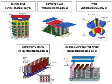
Figure 1: Today's polysilicon-based Monolithic 3D NAND Flash Memories.
The key points to note are:
- Lithography steps for patterning multiple memory layers are shared, which lowers cost.
- Polysilicon is used as the channel material for transistors.
- To be cost-competitive with scaled 2D NAND flash memory, aspect ratios to be etched and filled are often 50:1 or higher. For future generations, aspect ratios need to be increased further!
The questions to ask are therefore: Can we build 3D NAND flash memories with single crystal silicon instead of polysilicon? In addition, can we use low aspect ratios and still have cost-competitive products? I will now describe MonolithIC 3D Inc.’s technology, where both these important problems are solved. We were awarded fundamental patent coverage on this technology just a few months back.
Ion-Cut: The Building Block
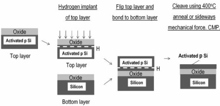
Figure 2: The Ion-Cut process can provide stacked single crystal silicon at low thermal budget.
Ion-cut, the technology used for manufacturing all SOI wafers nowadays, can provide stacked single-crystal silicon at low thermal budgets. Its shown in Figure 2. Ion-cut involves bonding a hydrogen implanted top layer wafer onto a bottom layer wafer, cleaving the bonded stack at its hydrogen implant plane and later polishing the surface. This process was invented in the early 1990s at CEA -LETI and has been in production since the late 1990s.The process costs around $60 per layer of memory, which is affordable. Ion-cut will become a public-domain technology in 2012, when its basic patent expires. For more cost information on ion-cut, please see my old blog post: How much does ion-cut cost?
Process Flow
Figure 3 describes the process flow for constructing our company's monolithic 3D NAND flash memory technology. The key point to note is how lithography steps for patterning multiple memory layers are shared, keeping cost per bit down. The memory cell is a double gate depletion mode single crystal silicon transistor that utilizes charge-trapping as the storage mechanism.
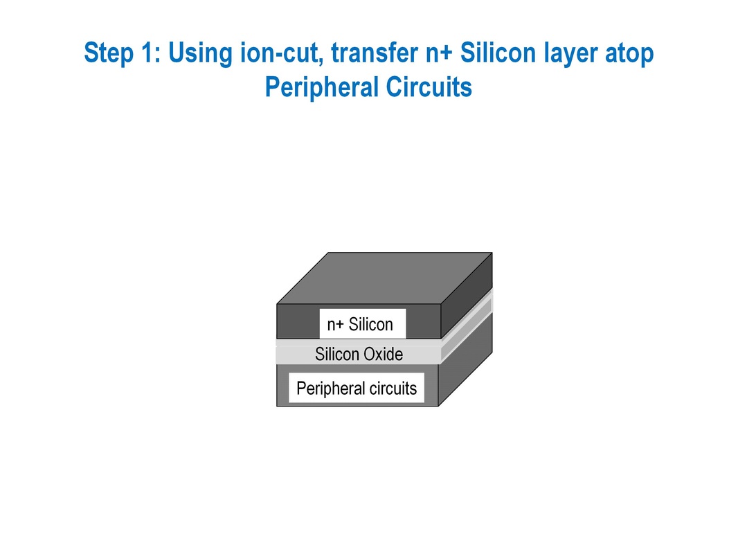
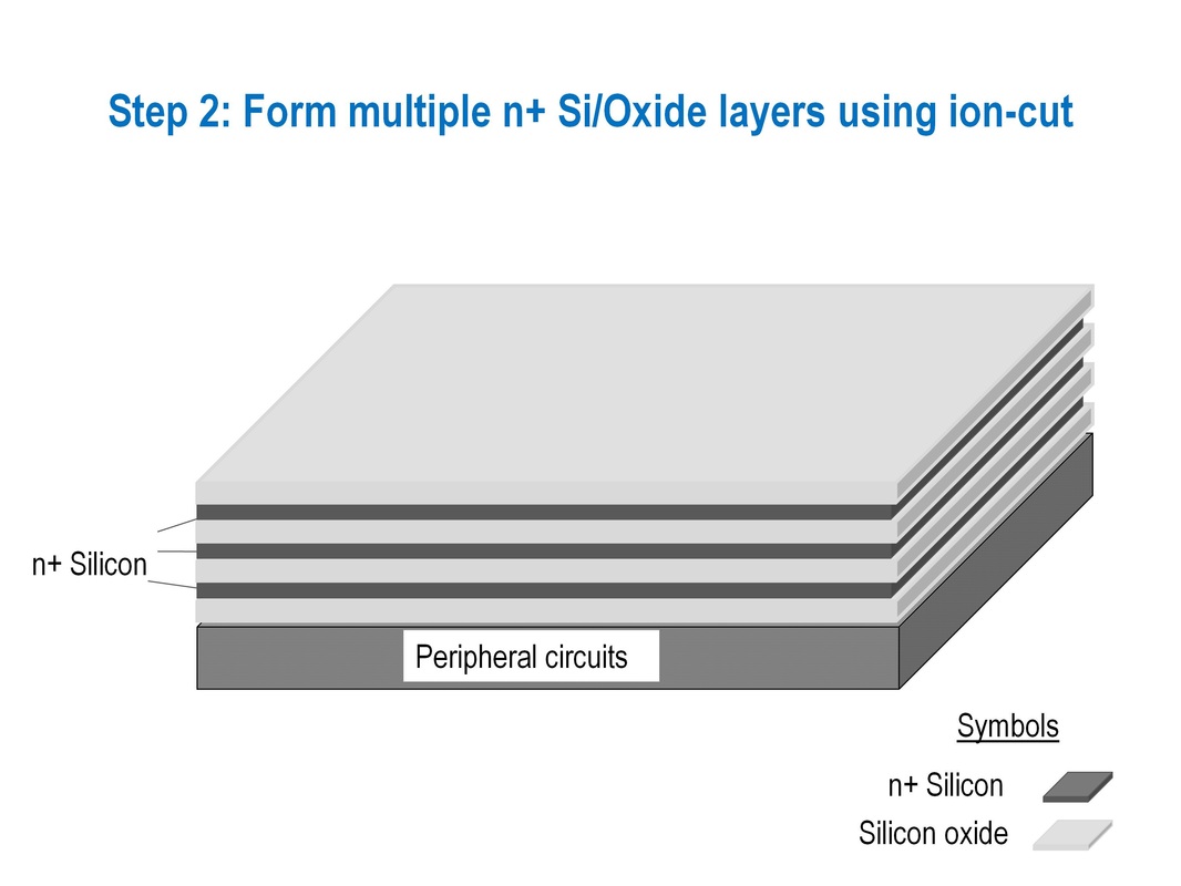
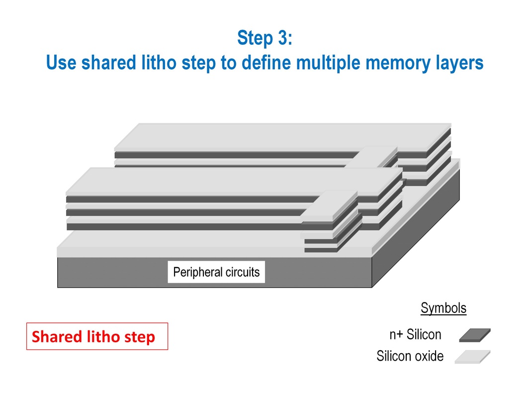

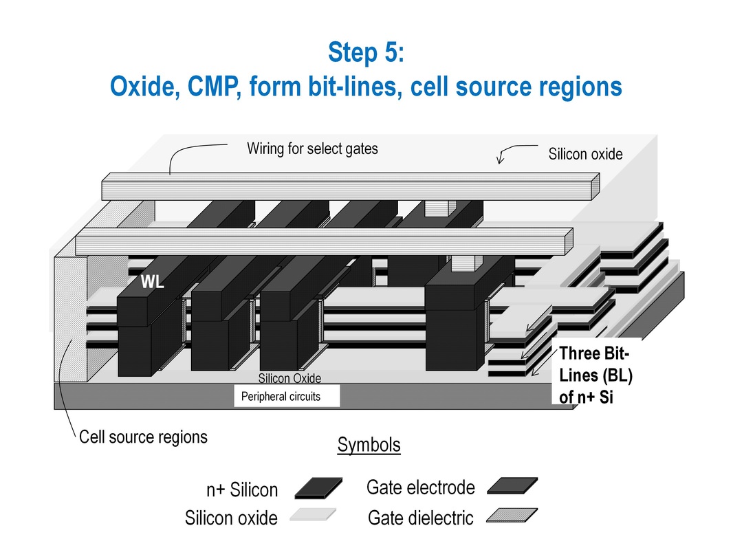
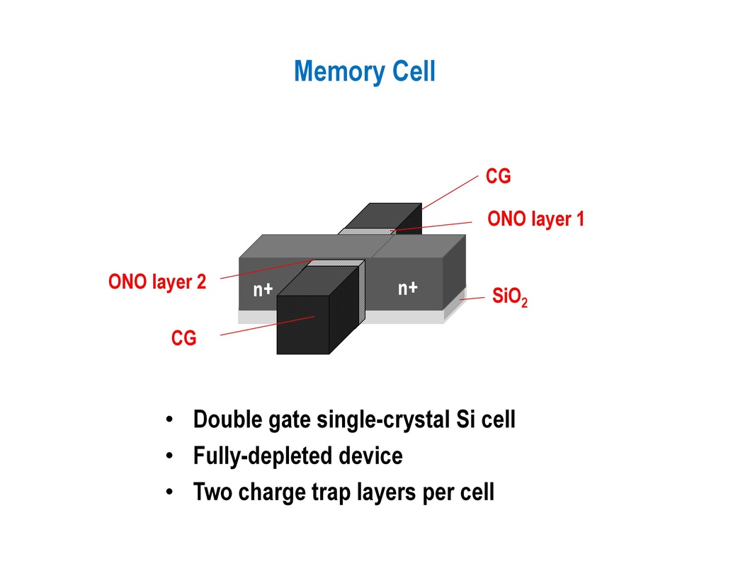
Figure 3: Process flow for constructing our company's Monolithic 3D NAND Flash Memories.
(Click on any of the above images to enlarge)
(Click on any of the above images to enlarge)
The steps involved in this process are:
- Step 1: Ion-cut is used to transfer a n+ single crystal silicon layer atop the peripheral circuits as depicted in Figure 3. Notice how the peripheral circuits are placed under the memory array... this improves array efficiency. Tungsten may be used for the wiring of the periphery.
- Step 2: Using steps similar to Step 1, a silicon-silicon dioxide multilayer sandwich is formed as described in Figure 3. A high temperature anneal may be conducted (if desired) to reduce defect levels in the layer transferred silicon.
- Step 3: Using the same litho and etch step, multiple layers of memory are defined.
- Step 4: Gate dielectrics and electrodes are formed for multiple levels of memory at the same time.
- Step 5: Cell source regions are formed. Contacts to multiple levels of memory are defined with shared litho steps using a process described in [Tanaka, et al., Symposium on VLSI Technology, 2007]. Figure 3 reveals the structure after this step. Using carefully chosen biases to bit-lines (BLs), word-lines (WLs) and the cell source, bits in the memory array can be accessed.
Implications
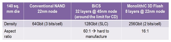
Figure 4: Estimates for density based on data presented at the 2010 VLSI Symposium Short Course.
Figure 4 gives estimates for density and aspect ratio based on data presented at the 2010 VLSI Symposium Short Course. MonolithIC 3D Inc.'s single crystal silicon solution can provide 4x higher density than conventional NAND flash memory at the 22nm node. Aspect ratios are manufacturable, unlike today's poly-based solutions.
Our technology is, of course, applicable to any monolithic 3D NAND flash memory architecture where the transistor's channel is horizontal. For more details, please check out our issued US patent #8,026,521 or contact me by e-mailing deepak@monolithic3d.com.
- Post by Deepak Sekar


 RSS Feed