
We have a guest contribution from Zvi Or-Bach, the President and CEO of MonolithIC 3D Inc. Zvi discusses the EE Times blog piece: Moore's Law Dead by 2022, Expert Says.
“Moore’s Law Dead by 2022” announces EE Times headline reporting Bob Colwell’s keynote at Hot Chips this week. Actual quote: "Moore's Law -- the ability to pack twice as many transistors on the same sliver of silicon every two years -- will come to an end as soon as 2020 at the 7nm node". Collwell told the audience that DARPA “tracks a list of as many as 30 possible alternatives to the CMOS technology that has been the workhorse of Moore's Law …My personal take is there are two or three promising ones and they are not very promising,". Colwell is the Director of DARPA’s Microsystems Technology Office (MTO) and has both visibility and credibility in these matters. In fact, this is not his first time to publicly state the end of Moore's Law -- he did so at ACM SIGDA and DAC meetings earlier this year. His slide (below) clearly presents the gap between the end of dimensional (Dennard) scaling and the establishment and ramp-up of alternatives to the current silicon based technology.
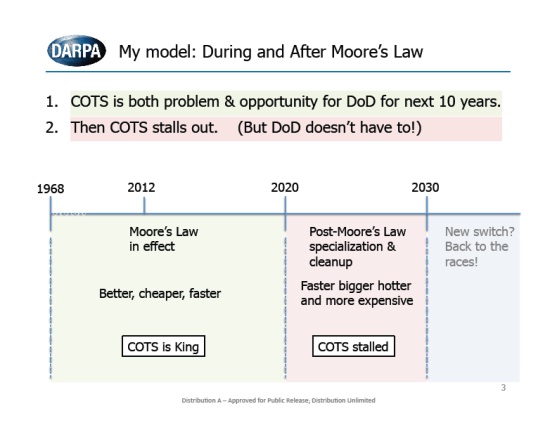
Figure 1
The discussion at EE Times remind us that we have "been hearing this for 20 years or more", so why is it different now? Well, even in the crying wolf story the wolf eventually did come! This time the signs are very clear. In fact, one could argue that as far as cost reduction, Moore's Law is already dead. The following ASML chart clearly shows it.

Figure 2
Taking into account additional information released during the recent Semicon West, it seems that effective cost for most fabless companies might even go higher with future scaling. Even if we ignore the fact that most foundries chose to keep their metal rules at 20nm when going to 14nm node, with the associated end-device cost implications, advanced nodes come with many additional layout restrictions. Those create circuit design and interconnect overheads that eat away a large part of theoretical scaling benefits. Quoting Andrew Kahng: "Constant area-factors allowed prior node scaling to be 2x, however since 2009 the real scaling has been 2E(2/3)x or ~1.6x due to an “IC Design Gap". Add to it the fact that embedded memory SRAM bit cell is expected to barely scale, as shown in the following slide, and end-product costs might go up even for the same SoC complexity!
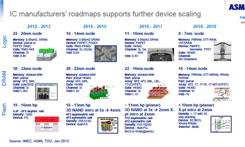
Figure 3
The following chart from Samsung clearly illustrates this dynamics for NAND, but from the above discussion it may be even more true for SoC.
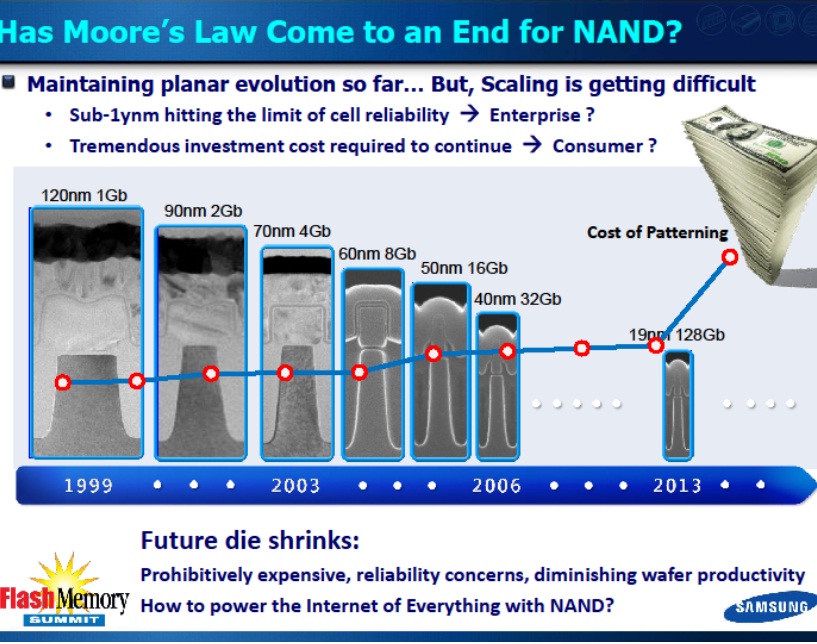
Figure 4
The issue of cost has very significant implications. For the semiconductor industry Moore's Law is not just a matter of pride: it became one of its fundamental business drivers. In the food industry vendors keep on selling food as it get consumed, clothing and car industry products get worn out or go out of fashion. But in the semiconductor industry old products mostly get displaced by better new products – the upgrades. Imagine what would happen to the major industry players’ stock if they were to update their projections to expect 20% reduction in revenue!!!
And 20% might be a conservative number once the dynamics of the last 30 years would hit a hard stop.
The following Samsung chart is a good illustration of where we are and the choice that at least Samsung has made:
And 20% might be a conservative number once the dynamics of the last 30 years would hit a hard stop.
The following Samsung chart is a good illustration of where we are and the choice that at least Samsung has made:
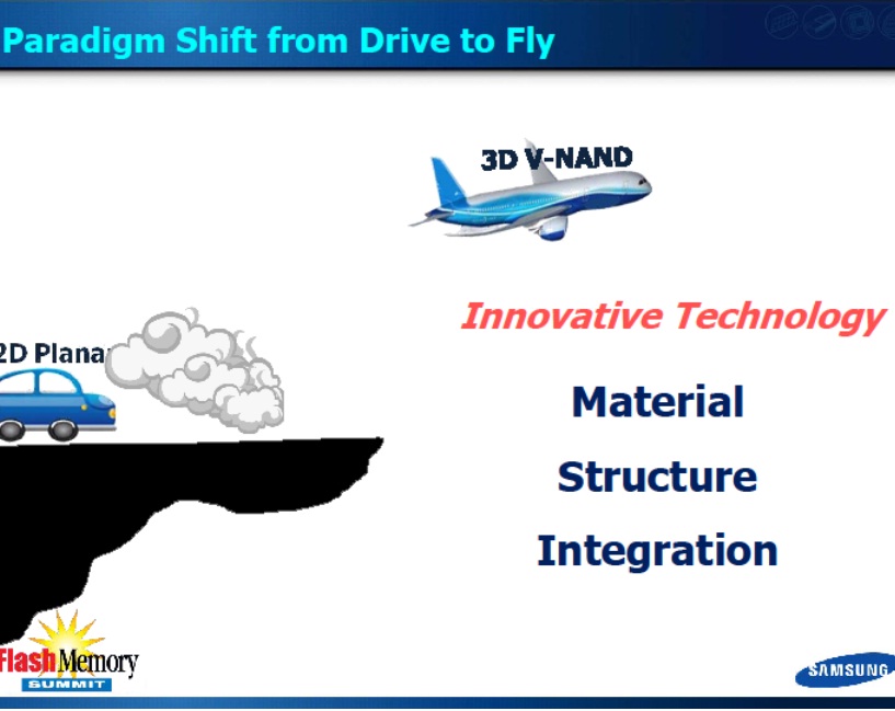
Figure 5
We can keep on hoping that the wolf will never come, just as it hasn't before. Or we can take action now before 'they comes'.
Samsung, Toshiba and the rest of the NAND industry are already taking action. On the SoC side the challenges are as severe, yet at this point the industry is consumed by the enormous efforts to bring up FinFETs. It may even bring up compound semiconductors (III-V) for the next node (10nm), but then what? At what cost? For what kind of return?
It seems to me that the right moves are:
First, logic design market needs to adopt an alternative to the embedded memory. IBM stated at the recent Common Platform Forum that adopting eDRAM gave it the equivalent benefit of one node scaling. This was seconded by Intel’s recent announcement of integrating eDRAM with their new Haswell processor - Intel eDRAM attacks graphics in pre-3-D IC days. An even better option would be the one transistor two state memory breakthrough solution recently developed by Zeno Semiconductors.
Second, logic design needs to follow the NAND industry by developing monolithic 3D technology for SoC and logic products. In a recent blog we reported that CEA Leti has placed Monolithic 3D is now on the roadmap for 2019. We are pleased to announce that we will provide a tutorial on monolithic 3D as a part of the upcoming IEEE 3D IC Conference in early October in San Francisco, and we will follow with a plenary talk the following week at the IEEE S3S Conference in Monterey. In these conferences we also plan to present a new practical process flow for monolithic 3D, leveraging industry’s shift to laser annealing. This technology supports 3D technologies we had presented in the past, and can be used independently for new monolithic 3D process flows. We are looking forward to meeting you all there.


 RSS Feed