Monolithic 3D Inc., the Next Generation 3D-IC Company
  • Home
  • Technology
    • Technology
    • Papers, Presentations and Patents
    • Overview >
      • Background
      • Why Monolithic 3D?
      • Paths to Monolithic 3D
      • Applications
    • Ion-Cut: The Building Block
    • Monolithic 3D Logic >
      • RCAT
      • HKMG
      • Laser Annealing
      • RCJLT
      • 3D Embedded RAM
      • 3D Gate Array
      • FPGA
      • Ultra Large Integration - Redundancy and Repair
    • Monolithic 3D Memory >
      • 3D DRAM
      • 3D Resistive Memories
      • 3D Flash
    • Monolithic 3D Electro-Optics >
      • 3D Image Sensors
      • 3D Micro-Displays
  • 3D-IC Edge
    • 3D-IC Edge
  • News & Events
    • News & Events
    • S3S15 Game Change 2.0 Video/P
    • Webcast
    • Webinar
    • Press Releases
    • In the News
    • Upcoming Events
  • About Us
    • About Us
    • History
    • Team
    • Careers
    • Contact Us
  • Blog
  • Simulators

Qualcomm: Scaling down is not cost-economic anymore - so we are looking at true monolithic 3D

6/17/2014

0 Comments

 
Picture
We have a guest contribution from Zvi Or-Bach, the President and CEO of MonolithIC 3D Inc. Mr. Or-Bach discusses about the latest news in support of monolithic 3d.

Over the course of three major industry conferences (VLSI 2013, IEDM 2013 and DAC 2014), executives of Qualcomm voiced a call for monolithic 3D "to extend the semiconductor roadmap way beyond the 2D scaling" as part of their keynote presentations.  
Karim Arabi, Qualcomm VP of Engineering, voiced the strongest support and provided many details of monolithic 3D’s role, in his keynote at this year’s DAC. A good summary was posted at the Tech Design Forums site under the title "3D and EDA need to make up for Moore’s Law, says Qualcomm". In this blog I’ll highlight some of the very interesting quotes from Arabi’s keynote: "Qualcomm is looking to monolithic 3D and smart circuit architectures to make up for the loss of traditional 2D process scaling as wafer costs for advanced nodes continue to increase...One of the biggest problems is cost. We are very cost sensitive. Moore’s Law has been great. Now, although we are still scaling down, it’s not cost-economic anymore"

Karim Arabi, Qualcomm VP of Engineering, voiced the strongest support and provided many details of monolithic 3D’s role, in his keynote at this year’s DAC. A good summary was posted at the Tech Design Forums site under the title "3D and EDA need to make up for Moore’s Law, says Qualcomm". In this blog I’ll highlight some of the very interesting quotes from Arabi’s keynote: "Qualcomm is looking to monolithic 3D and smart circuit architectures to make up for the loss of traditional 2D process scaling as wafer costs for advanced nodes continue to increase...One of the biggest problems is cost. We are very cost sensitive. Moore’s Law has been great. Now, although we are still scaling down, it’s not cost-economic anymore"

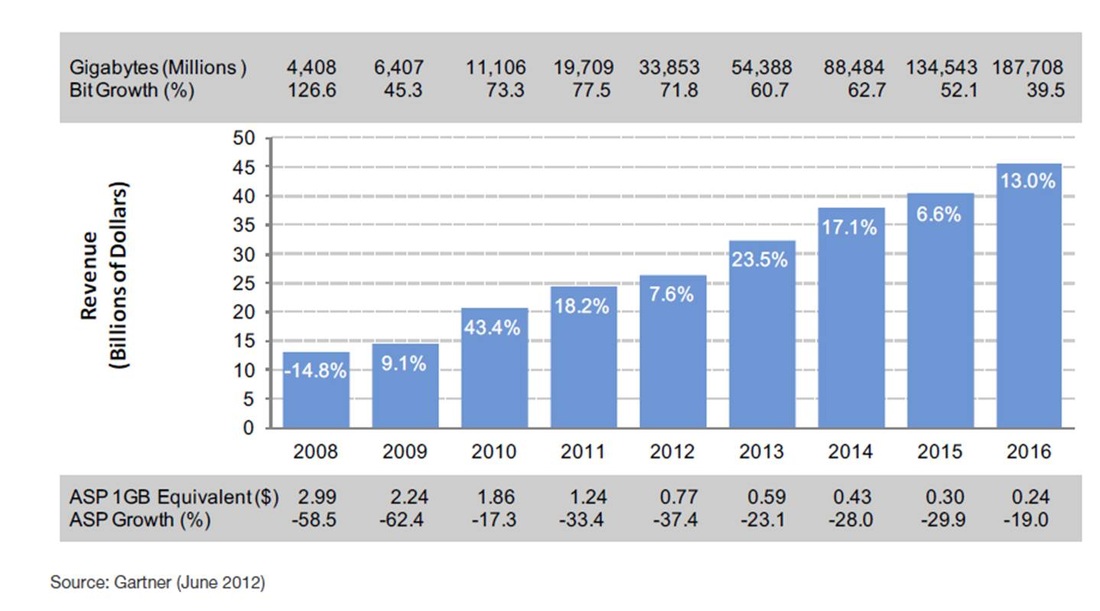
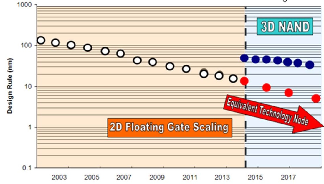
Qualcomm is not the only fabless company voicing its concern with cost. Early in 2013 Nvidia said it is "deeply unhappy" and executives of Broadcom followed suite. The following chart, presented by ARM, illustrates it nicely.
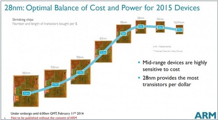
Picture
Figure 1
But it seems that the problem is even more severe than that. In our blog Moore’s Law has stopped at 28nm we examined the expected increase of SoC cost due to poor scaling of embedded SRAM (eSRAM). We should note that the chart above, like many others, is about the cost per transistor associated with dimensional scaling. Escalating lithography cost causes escalating wafer cost, which neutralizes the 2X transistor density increases.

Yet eSRAM scales far less than 2X and, accordingly, for most SOCs, scaling would be even more costly. This issue has been confirmed again with the recent VLSI 2014 paper "10-nm Platform Technology Featuring FinFET on Bulk and SOI" by Samsung, IBM, STMicroelectronics, GLOBALFOUNDRIES and UMC. They presented that the size of their 10 nm bitcell is 0.053 µm², which is only 25% smaller than the 0.07 µm² reported for 14 nm bitcell size. One should expect that an additional area penalty would occur for effective use in large memory blocks, as reported even for 14nm, which could bring the effective SRAM scaling to only about 15%, a long way from the 50% required to neutralize the escalating wafer costs. 

However, cost is not the only issue that forced Qualcomm to consider monolithic 3D. Quoting Arabi:
“Interconnect RC is inching up as we go to deeper technology. That is a major problem because designs are becoming interconnect-dominated. Something has to be done about interconnect. What needs to be done is monolithic three-dimensional ICs. Through-silicon vias and micro bumps are useful where you need I/Os ... But they are not really solving the interconnect issue I’m talking about ... So we are looking at true monolithic 3D. You have normal vias between different stacks. Then interconnect lengths will be smaller than with 2D. If we can connect between layers the delay becomes smaller." 

The interconnect issue was also addressed at IEDM 2013 by Geoffrey Yeap, Qualcomm VP of Technology, in his invited talk:
"As performance mismatch between transistors and interconnects continue to increase, designs have become interconnect-limited. Monolithic 3D (M3D) is an emerging integration technology poised to reduce the gap significantly between transistors and interconnect delays to extend the semiconductor roadmap way beyond the 2D scaling trajectory predicted by Moore’s Law."
Yeap provided the following chart for the growing gap between transistor delay and interconnect delay:
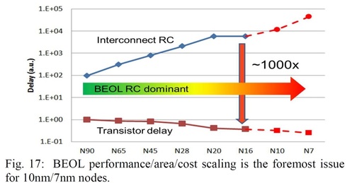
Picture
Figure 2
Arabi DAC 2014 keynote was also reported on Cadence’s website, which provides our final Arabi quote for this blog: Qualcomm is looking at "monolithic" 3D-ICs that use normal vias between stacked dies. This can provide a one-process-node advantage along with a 30% power savings, 40% performance gain, and 5-10% cost savings.

Clearly, monolithic 3D integration has a very important role in the future of the semiconductor industry. It is therefore fitting that the traditional IEEE conference on SOI has extended its scope and now calls itself S3S: SOI technology, 3D Integration, and Subthreshold Microelectronics. The 2014 S3S conference is scheduled for October 6-9, 2014 at the Westin San Francisco Airport. This would be a great opportunity to learn more about monolithic 3D technology, with 5 invited presentations covering topics from design tools to monolithic 3D NAND and other 3D memories. CEA Leti will present their work on CMOS monolithic 3D IC, and researchers from MIT and Stanford will present manufacturing monolithic 3D devices with materials other than silicon.
submit to reddit
0 Comments

EUV vs. TSV: Which one will become production ready first?

7/31/2013

1 Comment

 
Picture
We have a guest contribution today from Israel Beinglass, the CTO of MonolithIC 3D Inc. Israel debates on the answer to an important question that is on everybody's mind these days.

Like every Semicon West show in the past, where many experts are brought together for showing the latest and greatest semiconductor manufacturing equipment and bringing numerous seminar/panel discussions, this Semicon West of 2013 was no different. Two major issues were discussed, which on the face of it look unrelated, that caught my attention:

Progress in

  1. 3D - TSV technology, and
  2. EUV
Obviously these two issues are very different, but they are quite similar in respect to the following:

1. As the advanced node progresses to smaller and smaller feature size we are getting closer to the "end of the road map" or the "end of Moore's law".

Going to EUV does alleviate some of the problems related to the current solution of double patterning (or quadruple in the future assuming, EUV doesn't come to fruition soon enough).

As well, utilizing 3D devices with TSV has, in the grand scheme, a similar outcome; namely, advancing the integration via 3D structures rather than continued scaling. Though in the future, 3D devices and advanced nodes could go hand in hand.

2. The big miss of the road map. When one looks at some old road maps from a few years ago, one can ask how did we, the industry, miss by so much?

This actually reminds me of another miss from a few years ago-the low k inter-metal dielectric. Fig. 1 shows the low k dielectric roadmap trend of various ITRS published roadmaps and the prediction in 1999 that by 2004 we would be using k<2 !! Obviously we know what happened and even today 14 years later it is hard to breakthrough a k value of 2.5. 
Picture
Figure1: low k Dielectric Road Map
Figures 2 and 3 show the roadmap for EUV and TSV, respectively. Both are of 2009 vintage. In each case the prediction of the road map vs. actual is startling.
Picture
Figure 2: EUV road map
Picture
Figure 3: TSV road Map
It is not the purpose of this blog to go over the reasons why the roadmaps of EUV and TSV missed the time table by miles, nor to blame anybody for it. There are many articles and discussions published on the subjects. Rather, I will touch on some of the highlights as well as try to make some conclusions regarding the pathway of the industry regarding these two important technologies.

EUV: The EUV technology has so far gone through monumental achievements vis-à-vis the incredible tasks of developing the next generation stepper technology. The amount of engineering and resources poured into it is unprecedented in the short history of the semiconductor industry and maybe so for other industries.

It looks like as I write this blog that the only barrier for the technology from becoming a HVM tool is EUV source power that can provide a high enough throughput. Many experts doubt that it could ever be achieved; however, there are many other experts saying that it is within a reach.

TSV: In this case I could see two totally unrelated issues:

1. Technology driven obstacles

2. Logistics and supply chain issues.

In the case of the TSV it is one of the few cases where the "power point" presentation(s) of the TSV idea are so convincing that it is actually hard to oppose it. However, when it comes to the fine details of the technology development, there are many issues that still need to be addressed and resolved. I believe that it is just a matter of time before the technical obstacles will be resolved and a unified standardized solution emerges. However, on the other hand, I see a real problem from the point of view of logistics, cost and supply chain of the technology, and I have some doubts if it can ever be resolved. For further discussion on this issue, please refer to: 3D IC Supply Chain: Still Under Construction, and to a detailed comment in EE Time published blog and comments re. Semicon West 3D - IC TSV, provided here below.

In summary, I believe that the industry will come with a solution for EUV before TSV becomes a production technology.

Yet there is another alternative to TSV and to EUV - it is the Monolithic 3D methods. Moreover, it is very likely that monolithic 3D will reach volume production before EUV and TSV. As we already see the  NAND Flash vendors ramping up for production of 3D NAND.

The detailed comment fromm EE Times re. Semicon West 3D - IC  TSV:

PictureUSER RANK CEO
Re: Semicon Showed Support for 3D ICs  
chipmonk0   7/18/2013 1:46:13 PM

" same old same old ... " !! With such pollyannaish coverage, I am afraid that TSVs will remain the next hot interconnect tech even 5 years from now !

To provide a counter-point to all this happy talk, SemiCon had invited me to lead a 1 hr discussion at the Show on "Roadmap for TSVs and Alternatives from a Technology perspective ". Since Herb was not there, here are the key points :

1. unlike previous Advanced Packaging technologies like Flip Chip which we developed at IDMs like Motorola & Intel with both deep / broad expertise and product commitments, the development of TSVs has been going on mostly at overseas Govt. funded Laboratories in fits and starts and has then jumped to Foundries / OSATs. Xilinx' use of 2.5-d to integrate poorly yielding FPGAs has led to much irrational exuberance and then disappointment.

2. In the Winter of 2010 - 11 Samsung reported the first Wide I/O DRAM stack using TSVs. Great bandwidth even at 200 MHz & terrific power eff. But what the blogosphere neglected to report was that the yields were down in the mud and since then not much has been heard about Wide I/O from Samsung. Instead they keep bringing out conventional LP DDR at ever higher Clock Rates. JEDEC has actually postponed Wide I/O to 2015. 
3.  The development of TSV technology has been going on in Fabs who do not have to be sensitive to stress issues common in "thick film" type laminates / composites as is the case for filled vias. It is only now that they are waking up to it. Stress effects depend on the sq. of via dia., hence the new interest in shrinking them below 5 um. But integration & reliability problems ( at high Aspect Ratios both get worse ) have not been thought through. Moreover, Bonding stacked chips using the current method ( a sort of pidgin version of the technology I had invented nearly 20 years ago at Motorola for GaAs Power Amps that went into Cell Phones ) also introduces residual stress, affects electron mobility and shifts timing. 

4. While these slow-poke Govt. funded Euro Labs rediscover stress effects on device perf. and the perils of Cu metallurgy applied indiscriminately, there is at least one small Company outside Chicago that has already shifted to the non - obvious ( at least to these TSV-niks ) yet theoretically sound choice of using Tungsten ( a brittle and poor electrical conductor which can be compensated by Design but unlike Cu a close CTE match with Si ).

5. But thats not all Folks - this tiny Co. with just 3 PhDs and Physicists has also solved the biggest TSV integration problem thats keeping all these Labs and various Tool Vendors new to the game ( in Herb's Osterreich they love to build big complex "Maschine" - Physics be damned ) -- intent on optimizing their individual process steps ( e,g. back up wafer bond / debond ) at the risk of compromising the whole process -- awake at night.

6. We did cover more, e,g. as to how to get the electrical benefits of TSVs w/o actually having to drill holes in live Silicon, circuitry and packages that make it possible. We already have some of these Alternatives ( using the concept of Active Interconnects ) under development - especially for the very large Server & SmartPhone markets - and have started publishing.

7. TSV development is orders of magnitude more complex than Flip Chip and would benefit from the same type of brutal, theory-driven Program Management practiced at the world's largest semiconductor Co., but since they have money in the Bank to stay on Moore's Law and thus continue single chip solutions they don't need TSVs that badly. So unless there is a radical shake - up in the TSV programs "outside", incl. at the Foundries, the present slow pace of TSV development will persist.

Morale : give TSVs a fair chance, they need a respite from these overly enthusiastic bloggers, embarassingly out of their depth, and at Conferences lets not blather about Supply Chain Issues, the technical probems are not all solved yet
submit to reddit
1 Comment

3D NAND Opens the Door for Monolithic 3D

10/1/2012

2 Comments

 
Picture
We have a guest contribution today from Israel Beinglass, the CTO of MonolithIC 3D Inc. Israel discusses the opportunities of 3D NAND with Monolithic 3D.

NAND technology, which is a subset of NVM (Non Volatile Memory), was invented by Fujio Masuoka of Toshiba back in 1984. Flash memory was presented at IEDM1984 by Dr. Masuoka and his colleagues [1].  The following is a short quote from the original paper “the cell is programmed by a channel hot carrier injection mechanism similar to EPROM. The contents of all memory cells are simultaneously erased by using field emission of electrons from a floating gate to an erased gate in a FLASH (Hence the name FLASH)”.  

Masuoka came back to the IEDM in 1987 and suggested a Flash NAND structure [2].
Intel created the first commercial NOR type of Flash chips in 1988. For the next few years some major developments occur in the Flash arena:
  • In 1989, Samsung and Toshiba created a NAND flash memory.
  • In 1994, Compact Flash was invented and introduced by SanDisk.
  • In 1999, the SD memory card was released by a combination of SanDisk, Toshiba and Matsushita.
  • In 2001, the world’s first 1 Gigabit Compact Flash card was introduced.
From 2006 onwards, NAND became the most scaled of devices beating out the microprocessor devices (see Figure 1). The current state of the art is 20nm (2x) technology, as the world’s appetite for storage is still strong. Flash Cards, SSD, Smartphone and Tablets are the leading growing applications.
Picture
Figure 1: Flash Vs. Microprocessor design rules cross over
NAND memory as a true cross point array with the control gate on top of the floating gate and only one contact for a whole string of cells has the smallest memory cell size as shown in Figure 2 In addition, when one adds with the capability of MLC (Multi Level Cells) to NAND devices, the bit density dramatically increases.
Picture
Figure 2: NAND, circuit diagram and SEM pictures in x and y directions.
The NAND market has been continuously growing for the last several years. Figure 3 shows the NAND revenue and Gigabytes increase since 2008 and the forward projection for the years 2012-2016.
Picture
Figure 3: NAND Revenue and Gigabytes growth
As the NAND technology has been moving to smaller and smaller process nodes some serious problems, physical and electrical surfaced:
           Physical Limitations:
  • Pattern scaling - lack of EUV is a major issue
  • Structure formation, Figure 4 depicts a 27nm NAND cell that shows how close the cells are getting to each other, and how much the aspect ratio is getting out of hand. This is a limiter to obtaining high yield.
          Electrical Limitations:
  • There is an increase in cell-to-cell interference in the word lines.
  • Capacitive coupling ratio has decreased
  • Dielectric leakage has increased
The number of electrons on the floating gate has decreased dramatically so much so that a small fluctuation in the number on the floating gate can make a huge effect on the cell function. Figure 5 describes the scaling induced phenomenon.
Picture
Figure 4: A 27nm NAND cell structure
Picture
Figure 5: Number of electrons on the FG decreases for advanced NAND technology nodes
It is a common understanding among the experts that the current NAND technology will not be able to be scaled down to the 10nm node.

The solution for this dilemma is the 3D NAND, which was initially proposed by Toshiba at the 2007 VLSI Symposium [3]. Toshiba unveiled its Bit Cost Scalable (BiCS) technology. BiCS makes use of a “punch-and plug” structure and charge trap memory films. Toshiba has fabricated a prototype 32-Gbit BiCS flash memory test array with a 16-layer memory cell using 60nm design rules, see Figure 6. Hynix, Samsung and Macronix have also come with their versions of the 3D NAND.
Picture
Figure 6: 3D NAND process steps, as described by Toshiba
The following are the key advantages of the 3D NAND:

  • With 3D NAND, scaling is no longer driven by lithography. The gate length is defined by deposition
  • The key steps to 3D NAND are
                                        - Build a multitude of oxide/nitride or oxide/doped polysilicon stacked layers
                                - Fill the deep memory holes or trench slits. The top foreseeable challenges are ultra-high-aspect ratio (>40:1) conductor etch and dielectric etch with high etch selectivity to the hard mask
  • 3D NAND is relatively straightforward for a DRAM maker since it has stacked SiO2 and polysilicon layers like a stacked capacitor DRAM, and trenches like a trench cell DRAM. 
  • 3D NAND is evolutionary, not revolutionary. 
  • The good news is continued cost reduction, smaller die sizes and more capacity. 
  • Installed NAND toolsets in the wafer Fabs can, for the most part, be reused, thereby extending the useful life of Fab equipment. 
  • 3D NAND technology is still basically NAND with all its inherent limitations of data reliability and performance: hence, generally well understood (evolutionary).
At this point all the NAND companies are putting a lot of effort to bring this process to high volume manufacturing; the current expectations are that in 2014-2015 it will be ready for prime time. 3D NAND will be a technology that will take us between the 2D planar NAND and whichever post-NAND technology emerges in the future.
Picture
Figure 7: 3D NAND effect on design rules
Figure 7 describes the essence of the advantage of moving from 2D to 3D NAND. The adoption of 3D NAND technology will remove the burden from the Litho (and hence EUV) into the much easier process steps (deposition). Of course there are other advantages as described above.

It is not too difficult to see the similarity between the up and coming 3D NAND and the Monolithic 3D approach. As we describe in our web site (www.monolithic3d.com) the advanced technology patented by MonolithIC 3D Inc. enables the fabrication of Monolithic 3D Integrated Circuits with multiple stacked transistor layers and ultra-dense vertical connectivity. Thus, it appears monolithic 3D-ICs with 2 device layers provide benefits similar to a generation of conventional scaling. Furthermore, just as conventional scaling reduces feature sizes every generation, monolithic 3D opens the road for many years of continuous scaling by ‘folding’ once, twice, and so forth without necessarily reducing feature sizes.


  1. F. Masuoka et. al IEDM 1984 pp464-467
  2. F. Masuoka et. al IEDM 1987 pp552-555
  3. H. Tanaka et al., Symp. on VLSI Tech. Dig., pp 14-15, 2007
submit to reddit
2 Comments

Intel vs. the Foundries: where is advanced logic heading?

6/4/2012

2 Comments

 
Picture
We have a guest contribution today from Israel Beinglass, the CTO of MonolithIC 3D Inc. Israel discusses about Intel vs. Foundries. 

Do real men need to have a fab?
Will Apple and Qualcomm become IDMs?


A lot of turmoil recently arose over the lack of TSMC capacity to support the 28nm logic ramp. Some of the larger TSMC customers such as Qualcomm and Nvidia made public their disenchantment with TSMC’s delivery of 28nm products.

Let’s try to put things in order and analyze the situation thoroughly, especially from the point of view of process capabilities and performances. There are obvious differences between what Intel does and what the foundries do. For this discussion we will use TSMC to represent the foundries. Both companies, Intel and TSMC, are making logic devices so we can compare their respective capabilities in the logic arena. For the last few decades Intel has been the leader in the area of process technology with the introduction of several process innovations as shown in Figure 1.
Picture
Figure 1: Intel innovation in process technology for the last decade (Intel web site)
For the most of the generations, the rest of the crowd has been trying to catch up with Intel. Sometime they are doing it within one node but other times they are not that successful and it takes several nodes to catch up.

Figure 2 is Intel’s view of the gap between them and the foundries, which I mostly agree with.
Picture
Figure 2: Intel’s leadership over foundries and other IDMs (Intel development forum 2012)
It is very clear that Intel is the “king of process” and leads the rest of the industry by leap and bounds. In a way it is somewhat not a fair competition for the following reasons:

Intel:
          A “one product company”, it is a company that thrives on the PC market with the high performance family of the microprocessors (including servers) as their main product line.
       It is well known that their efforts into mobile devices has not (yet) been successful, even with the billions of dollars already invested.
          The process technology machine is second to none; nobody can even get close to Intel’s transistor performance.
          The foundries are continuously trying (unsuccessfully) to catch up with Intel

TSMC (as representing the foundries):

            Running many different devices with multiple technology nodes and wafer sizes
            Running hundreds of different products where some are high volume runners and some run only a handful of wafers per year.
           Adjusting the process parameters for many of the products so that the yield will be optimum for each one of them. This could be a nightmare for an efficient fab operation…very different than what Intel is running in their fabs.

As mentioned at the beginning, an interesting situation has emerged within the last few months; the so called “the 28nm foundry crisis”. The situation came from an unforeseen huge demand for the just-introduced-to-production 28nm process. It is an unprecedented situation where the demand for a new node outstrips the current supply. All of the foundries are scrambling to increase production in order to satisfy the unhappy customers.
Here are some quotes to that effect by some of the major players.

  •          Qualcomm: “We are seeing very strong demand for our industry-leading Snapdragon 4, MSM8960, and other 28nm products,” Qualcomm's CEO Paul Jacobs told press and analysts during the company's earnings call late yesterday. 'Although the manufacturing yields are progressing per expectations, there is a shortage of 28nm capacity.
  •       Nvidia Corp’s CEO Huang: …“besides continuously increasing capital expenditures that the company ran into in the recent months will be accompanied by lower than expected gross margins in the forthcoming quarter”. The company blames low yields of the next-generation code-named Kepler graphics chips that are made at TSMC’s 28nm node. 
  •        Mark Bohr, who is the director of process architecture & integration and senior fellow of technology and manufacturing group at Intel, told EETimes that “the foundry model is collapsing. Chipmakers like Qualcomm will not be able to use TSMC’s single 20nm process”.
All of the major foundries are scrambling to add 28nm capacity:
            TSMC: Producing 28nm in Fab 14(Phase 4, 5) and Fab 15 (phase 1, 2). Planning to move Fab 15 (phase 3, 4) to 28nm by the end of the year
            GlobalFoundries: Running 32/28nm process in their Dresden fab and plan to move production on 32/28nm in their new Fab in Malta, NY
            UMC: Ramping 28nm in their Fab 12A (phase 3, 4)
           Samsung: The Korean Fab S1 is ramping 28nm production and rumors are that they will be converting line 14 (NAND Fab) to 28nm logic as well as the Austin NAND fab.
Several issues need to be addressed from this fiasco:

  1. What happened? Why this big and sudden capacity crunch?
  2. Are we setting ourselves up for a glut in 28nm capacity in 2013?
  3. Is some of the demand a result of double booking – a well known disaster in the making….
  4. Are Qualcomm and Apple going to be so disgusted with the situation that at the end of the day they will decide to follow the former AMD CEO Jerry Sanders’s saying “Only real men have fabs”?
My assessment to these 4 items is the following:

1.    The foundries fell asleep at the switch when they misread the advanced technology that Intel was bringing up and that their main customers needed the performance that the 28nm brings. Also the big fiasco of gate first vs. gate last on HighK metal gate and the long time it took for them to understand and execute this new process (some are even still using the inferior oxide/poly gate).

2.    It is typical to our industry (see the DRAM history) that when there is a shortage in one type of device/technology everybody is jumping the gun and increase production in an uncontrolled manner trying to capture more volume. At the end of the day there will definitely be an oversupply.

3.    Rumors are because of the situation that there already is double booking (sounds familiar….)

Both Apple and Qualcomm can afford with all the cash they are sitting on to have their own fabs to mitigate this kind of disaster…Will they do that? I personally doubt it. It is uncharacteristic to their business practice: however, depending on underperforming foundries is not a desirable situation.
As for the future, the situation is not getting easier. Intel has already announced and started high volume production of the new 22nm using FinFET (Tri Gate) transistor, a whole new concept for a production transistor structure.
Would the foundries be ready for that or we will again see fumbling around the issue? Do we really need FinFET at 22(20) nm or not?
submit to reddit
2 Comments

Is TSV for real?

4/8/2012

0 Comments

 
Picture
We have a guest contribution today from Israel Beinglass, the CTO of MonolithIC 3D Inc. Israel discusses about TSVs. 

Have you read some of the recent TSV headlines?

1. January 31, 2012 - CEA-Leti launched a major new platform, Open 3D, that provides industrial and academic partners with a global offer of mature 3D packaging technologies for their advanced semiconductor products and research projects.

2. March 7, 2012 - Semiconductor fab equipment supplier Applied Materials Inc. (AMAT) opened the new Centre of Excellence in Advanced Packaging at Singapore's Science Park II with its partner in the endeavor, the Institute of Microelectronics (IME)

3. March 26, 2012 - PRNewswire - Semiconductor design/manufacturing software supplier Synopsys Inc. (Nasdaq: SNPS) is combining several products into a 3D-IC initiative for semiconductor designers moving to stacked-die silicon systems in 3D packaging.

It is amazing that after so many years of development and efforts and great presentations we are still not in a full production and still basic R&D as well as EDA still in infancy.

Most people in the Industry consider Merlin Smith and Emanuel Stern of IBM the inventors of TSV based on their patent “Methods of Making Thru-Connections in Semiconductor Wafers” filed on December 28, 1964 and granted on September 26, 1967, as shown below patent  number 3,343,256
Picture
Figure 1: IBM TSV patent
In April 12, 2007 IBM announced a breakthrough new 3D technology:
Armonk, NY - 12 Apr, 2007: IBM (NYSE: IBM) today announced a breakthrough chip-stacking technology in a manufacturing environment that paves the way for three-dimensional chips that will extend Moore’s Law beyond its expected limits. The technology – called “through-silicon vias” - allows different chip components to be packaged much closer together for faster, smaller, and lower-power systems… IBM is already running chips using the through-silicon via technology in its manufacturing line and will begin making sample chips using this method available to customers in the second half of 2007, with production in 2008.
Picture
Figure 2: Original story on TSV advantages followed IBM announcement
Figure 2 is taken from Ignatowski’s presentation made shortly after IBM’s TSV announcement. This type of argument where chip stacking is compared to 2 chips side by side has become the corner stone of the TSV story (http://www.sematech.org/meetings/archives/3d/8334/pres/Ignatowski.pdf).

Already at that point (2007) it was clear to IBM that there were many issues with the technology that needed to be resolved.  Figure 3 shows the IBM slide discussing some of the problems for implementing TSV for mass production.
Picture
Figure 3: Issues per IBM with the TSV technology
During the years following and through to today there have been many attempts to bring the technology to the mass production. All have been without real success. 
The professional literature is full of beautiful road maps showing how TSV is going to change the industry with “more than Moore” as the next scaling methodology. 
Figure 4 is the Advanced Packaging road map for Texas Instruments which is typical of most companies Packaging/TSV road maps.
Picture
Figure 4: TI Packaging Technology Trends Dec 2011
There are several issues that are facing the industry when trying to implement TSV technology: (not in any specific order)
Process issues:
  • Via etching and filling are extremely slow since the dimensions are very different from the “normal” dimensions the industry uses (single/multiple digit microns for depth and diameter vs. nanometers, plus aspect ratios>5)
  • Via, first, middle or last which way to go? Each affects the whole process logistics in differing ways
  • How to integrate wafers from different sources Logic from IDM and/or foundry and memory from a memory Fab
  • Wafer thinning, how to handle fully processed wafer 20-80 micron thick including bonding and de-bonding. Rumors are that both Applied Materials and TEL are developing this kind of a tool
  • Wafer-to-wafer (W2W) or die-to-wafer (D2W) bonding: each  have processing challenges
  • Singulation of the final product
  • Substrate (carrier)for TSV

Design and EDA:
  •  Design rules are currently not compatible with TSV
  •  Who is responsible for the “system” design if there are several sources for product to be integrated?
  • EDA is way, way behind
  • Thermal simulation and heat removal issues
Back end issues:
  • Foundries/IDM vs. OSAT, who is doing what and who picks up yield loss
  • Final test
  • Reliability
  • The major foundries have no memory knowledge or how to integrate the memory on top of logic
Cost:

            - Currently the cost associated with implementing TSV is at least for now higher than other solutions. This is hampering the motivation to develop and implement the TSV technology.

Also the CapEx to implement TSV needs to be addressed, Figure 5 is a table put together by ASE that shows the readiness of the various equipment needed to run a typical TSV process.
Picture
Figure 5: TSV equipment readiness per ASE
One of the key issues that some people are neglecting right now is the fact that we do have an interim solution to the problem. It may- probably not be the best solution and perhaps not the most elegant one but it does work. These are the variety of packaging techniques using chip on chip with wire bonding, and assortment solutions (PoP etc).
Picture
Figure 6: Alternative methods for 3D chip connectivity
The following are some of the comments made by industry experts over the last few months.

TSMC
Doug Yu’s keynote address at the 3D Architectures for Semiconductor Integration and Packaging Conference in December, he noted that TSMC intends to provide full 2.5F and 3D service including chip design and fabrication, stacking and packaging. Yu, who is senior director of integrated interconnect and packaging, R&D at TSMC, outlined the key technologies that offer the best path to commercializing 3D integration technologies, with the implication that TSMC is well positioned to provide them all.

(http://www.infoneedle.com/posting/100745?snc=20641)

“TSV is much more complex and challenging than ever before,” noted Yu. “There’s a new ballgame and a small window.” He said a conventional collaboration infrastructure is becoming harder. Integration must be simplified to reduce handling and an investment beyond conventional back-end (in other words, middle-end-of-line tools and processes) is required. In short, Yu said a full spectrum of expertise is needed that includes manufacturing excellence, capacity and customer relationships where there is no competition with the customer 


Hynix
Nick Kim VP of Packaging  announced that for Hynix, production of 3D devices is no longer a matter of if but when and how (http://www.infoneedle.com/posting/100669?snc=20641)

Kim provided a detailed cost breakdown illustrating why 3D TSV stacks are more expensive (1.3x more) than wire bond stacks to manufacture. Overall, TSVs alone add 25% to the manufacturing cost because there is additional cost at each step:  

  •  Design: net die area decreases due to TSV array. 
  •  Fab: increased process steps due to TSVG formation, and capex for TSV equipment. 
  •  Packaging: Bumping, stacking, low yield and CapEx for backside processing equipment such as temporary bond and de-bond. 
  • Test: Probe and final package test time is increased because of the need to test at each layer as well as final. 
  • Hynix 3D roadmap: volume TSV production will officially start after 2013:
  • DRAM on Logic for mobile applications in a known good stacked die (KGSD) driven by form factor and power, are in development in 2012 with low production expected early 2013 ramping to volume late 2014. 
  • DRAM on interposer in a 2.5D configuration for graphics applications, driven by bandwidth and capacity is in development in 2012 with low production expected by the end of the year and ramping to HVM early in 2014. 
  • 3D DRAM on substrate for high performance computing (HPC) driven by bandwidth and capacity is in development in 2012, with low production expected early 2013, ramping to volume late 2014. 

In terms of supply chain management, Kim sees Hynix favoring the open ecosystem where logic and memory prepared with/for TSV from foundries and IDMs going to OSATs for assembly.

Overall it looks almost like a nightmare to implement TSV in a manufacturing facility. Even if all the processes steps will be taken care of, the logistics and co-ordination with different Fabs and OSAT are definitely no fun!!!

It looks like when we sum all the issues regarding the TSV methodology for achieving 3D, the approach of monolithic 3D suggested by MonolithIC 3D could resolve many of these issues and offer a far greater cost/performance gain from going 3D. Most of these advantages were already discussed in previous blogs and are part of the company web site,

Just few items that I would like to highlight:
  •  Practically no limit on the amount of vias between the different chips in the stack.
  • No deep TSV – nanometers, not microns!
  •  All done within the IDM or the foundry – better yield control & ramp, and no pointing fingers.
Please comment and let’s get a discussion going.
submit to reddit
0 Comments

Semiconductor Equipment Manufacturing - Who wins from the recent consolidation

2/27/2012

3 Comments

 
Picture
We have a guest contribution today from Israel Beinglass, the CTO of MonolithIC 3D Inc. Israel discusses about the semiconductor equipment manufacturing: "Who wins from the recent consolidation?"

2011 was a big year for consolidation in the semiconductor equipment manufacturing industry. The year started with the Varian acquisition by Applied Materials and was ended with the merger announcement of Novellus and Lam Research (not concluded when this blog is written).

The equipment business is relatively conservative and for many years only few noticeable successful M&A were done. Few past M&A were of a strategic nature. In these cases a large corporation buys a smaller one to either develop a product line or to buy into a growing product line. Table 1 is a snapshot of some past M&A activities in the short history of the semiconductor equipment industry-by far not a complete list.
Picture
Table 1 - Past M&A activities
As one can see many of the M&A turned to be a failure and became a big drain on the acquirer balance sheet. In several cases the company seized operation of the acquired company after several years, in other cases it is still going on with a moderate or very limited success. To mention two cases of a real success I can point to the Veeco acquisition of the MOCVD from Emcore and the merger of KLA with Tencor. In both cases the M&A dramatically boosted the company’s position, market cap and market share.

Going back to the two recent M&A namely Applied Materials Varian and Lam Novellus the question is how this will affect the semiconductor industry and who is going to benefit from it.

I definitely view these two activities in a positive way.

1.   Applied Materials and Varian: Looks like Varian had practically all the implant market and really didn’t have any room to grow (beside the new solar implant business-highly speculative). So selling the company to Applied Materials helped a lot… the employees and the top executives that suddenly got their stock price almost double…From Applied Materials point of view they now controlling most of the front end equipment and can influence the transistor technology more than before. Though I might emphasize as I mentioned in a previous Blog that the percentage of the implant business in the whole semi CapEx pie is shrinking in the last few years and probably with the introduction of the FINFET-Tri gate it will shrink even more. Still for Applied strong position in the Epi, RTP and Implant market they do have good position in the front end. The missing link of course is a good position in the ALD technology (controlled by ASMI).

In other hand customers don’t like to see too much power at the hand of one equipment vendor; they do like to see competition. Not clear how it will be played in the implant arena since no other real competitor in the horizon.

2.   LAM Novellus: This merger was proposed many years ago and almost every year was rumored to go through without actually happening to the dismay of analysts and others. However eventually it did happen! By combining the winning position of Lam in the etch and Novellus in the CVD the new combined company could expand and offers new modules and combinations of products especially in the back end and in the emerging double (quadruple) patterning that becomes a very important module in the advanced lithography.

In order to complete this discussion we need to look at the future, and in the future new technology of 3D devices will become a reality. Let’s discuss now how these M&A will affect the new world of 3D devices.

  1. TSV
    1. No real effect from the Applied Materials Varian deal since the implant is only a front end technology. Not clear if the Plasma Doping (PLAD) that supposes to do material modifications has any impact in the back end.
    2. For the Lam Novellus deal it could enhance the TSV technology since they could bring a more comprehensive solution to the TSV module that will include the etching, deposition and Cu plating. Of course they are missing the market leading position that Applied Materials has in the Cu barrier seed PVD equipment.
  2. Monolithic 3D
    1. Since Applied Materials own now the implant business they could easily get involved in the smart cut technology from point of view of proliferate it to the rest of the world, as it is currently dominate only by the SOI wafers manufacturing. Owning the RTP and Epi helps well in the Monolithic 3D module.
    2. No real effect from the Lam Novellus deal.
    3. The future introduction of Monolithic 3D technology into the Fab present an opportunity to all the equipment manufacturing companies from several new tools that need to be proliferate into the process flow.
submit to reddit
3 Comments

Do Foundries Have Too Much Power?

12/8/2011

4 Comments

 
Picture

We have a guest contribution today from Israel Beinglass, the CTO of MonolithIC 3D Inc. Israel discusses the foundry industry's history as well as its current landscape...


Read More
4 Comments

What’s wrong with the Semiconductor Equipment Manufacturing? - Part II - Where is the future growth?

11/3/2011

0 Comments

 
Picture

We have a guest contribution today from Israel Beinglass, the CTO of MonolithIC 3D Inc. Israel was at Applied Materials for almost two decades, and served as Chief Technology Officer and Chief Marketing Officer for many groups there.


Read More
0 Comments

What’s wrong with Semiconductor Equipment Manufacturing? - Part I

9/22/2011

10 Comments

 
Picture

We have a guest contribution today from Israel Beinglass, the CTO of MonolithIC 3D Inc. Israel was at Applied Materials for almost two decades, and served as Chief Technology Officer and Chief Marketing Officer for many groups there.


Read More
10 Comments

Accelerating Moore's Law

8/25/2011

0 Comments

 
Picture

We have a guest contribution today from Israel Beinglass, MonolithIC 3D Inc.'s CTO. Israel talks about how 3D technology can accelerate Moore's Law by providing more than 2x transistor density every two years.


Read More
0 Comments
<<Previous

    Search Blog


    Meet the Bloggers


    Follow us


    To get email updates subscribe here:


    Recommended Links

    3D IC Community
    3D IC LinkedIn Discussion Group

    Recommended Blogs

    • 3D InCites by Francoise von Trapp
    • EDA360 Insider by Steve Leibson
    • Insights From the Leading Edge by Phil Garrou
    • SemiWiki by Daniel Nenni, Paul Mc Lellan, et al.

    Archives

    March 2022
    December 2021
    August 2021
    August 2018
    July 2018
    May 2018
    October 2017
    September 2017
    December 2016
    September 2016
    August 2016
    November 2015
    October 2015
    September 2015
    July 2015
    June 2015
    May 2015
    April 2015
    March 2015
    February 2015
    October 2014
    September 2014
    August 2014
    July 2014
    June 2014
    May 2014
    April 2014
    March 2014
    February 2014
    January 2014
    December 2013
    November 2013
    October 2013
    September 2013
    August 2013
    July 2013
    March 2013
    February 2013
    January 2013
    December 2012
    November 2012
    October 2012
    August 2012
    June 2012
    May 2012
    April 2012
    March 2012
    February 2012
    January 2012
    December 2011
    November 2011
    October 2011
    September 2011
    August 2011
    July 2011
    June 2011
    May 2011
    April 2011
    March 2011

    Categories

    All
    3d Design And Cad
    3dic
    3d Ic
    3d Nand
    3d Stacking
    3d Technology
    Brian Cronquist
    Dean Stevens
    Deepak Sekar
    Dram
    Education
    Heat Removal And Power Delivery
    Industry News
    Israel Beinglass
    Iulia Morariu
    Iulia Tomut
    Monolithic3d
    Monolithic 3d
    MonolithIC 3D Inc.
    Monolithic 3d Inc.
    Monolithic 3d Technology
    Moore Law
    Outsourcing
    Paul Lim
    Repair
    Sandisk
    Semiconductor
    Semiconductor Business
    Tsv
    Zeev Wurman
    Zvi Or Bach
    Zvi Or-Bach

    RSS Feed

© Copyright MonolithIC 3D Inc. , the Next-Generation 3D-IC Company, 2012 - All Rights Reserved, Patents Pending